100 Gb/s Physical-Layer Testing Tips and Tricks
Driven by on-demand video, cloud applications, social sharing, and much more, today’s always-connected world has an insatiable craving for more bandwidth. With 10 Gb/s and 40 Gb/s falling to the wayside, the focus now is on deploying 100G, typically composed of four 25 Gb/s electrical channels feeding 100G optical transport systems.
Behind the scenes, advances in high-speed serial are making this possible. Noise-resistant differential signaling, jitter-resistant embedded clocking, and closed-eye equalization are among the breakthroughs that enable 25+ Gb/s on previously inconceivable trace lengths on circuit boards. The use of four 25G links (compared to 10 links at 10 Gb/s) simplifies 100G signal transmission to optical transceivers. The result is that many datacom and telecom technologies are using 100 Gigabit Ethernet (100 GbE) for transport, including SAS, Infiniband, and Fibre Channel. The rise of Ethernet is quickly replacing venerable SONET/SDH.
While the rush to deploy 100G technology is in full swing, the industry still is trying to perform more efficient testing at 25+ Gb/s rates. This means designers need to understand how analog waveforms relate to digital signal bit error rates (BER). Consider this: a bit period at 25 Gb/s is just 40 ps. The jitter budget has all but disappeared. Less than 3 ps of random jitter (RJ) close the eye altogether, and emerging standards typically permit less than 700 fs of RJ. This places emphasis on the intrinsic jitter and noise of the measurement instruments used to evaluate the signaling.
Every 25+ Gb/s high-speed serial technology shares common themes, but there are differences among the various standards. When there are gaps, it’s best to fall back on the Implementation Agreements of the Optical Internetworking Forum’s Common Electrical Interface (OIF-CEI). Common themes across the standards typically revolve around the interplay of jitter, noise, and crosstalk.
Emerging 100 Gb/s and Related Standards
As is often typical, market demand is ahead of standards. Since most of the test specifications have not been published, the details summarized in Table 1 are typical of what to expect. However, for compliance testing, be sure to check the actual standards for specific numbers as they become available.
Standards marked with an asterisk have not been released; consider the values speculative.
The two most established 100-GbE optical transmission specifications, both covered in IEEE 802.3ba, are long-reach 100GBASE-LR4 and extended-reach 100GBASE-ER4. The differences between them are primarily at the receive end. The ER4 receiver has greater sensitivity and must pass a more difficult stress tolerance test than the LR4 receiver.
The short-reach 100GBASE-SR4 4×25 Gb/s low-cost, multimode (MM) standard along with those for electrical transport over cables and backplanes, 100GBASE-CR4, and 100GBASEKR4 are works in progress. When finished, the 100GBASE specifications will provide a complete suite of optical interconnect systems.
Implementation agreements (IAs) from the OIF-CEI do not prescribe compliance tests the way that IEEE 802.3ba 100 GbE or Fiber Channel specifications do. Instead, the emphasis is on informative and normative tests that attempt to assure component interoperability across standards. Normative tests are like compliance tests in the sense that the committee prescribes them to assure interoperability; informative tests are recommended to develop a more thorough understanding of performance and margin.
The short-reach IA OIF-28G-SR consists of multiple lanes at 19.90 to 28.05 Gb/s of differential pairs over 300 mm of PCB with up to one connection operating at BER < 10-15. The very short reach IA OIF-28G-VSR has not been published, but a preliminary version is available. It consists of multiple electrical lanes at 19.60 to 28.05 Gb/s for signaling between Serdes (called hosts in the IA) and transceivers (modules in the IA). The Serdes and transceiver can be separated by about 100 mm of PCB to a connector plus an additional 50 mm or so of conducting trace. The system is required to operate at BER < 10-15.
The high-rate Fibre Channel standard, 32GFC, has a data rate of 28.05 Gb/s. The confusing name scheme comes from the desire for the name of each generation to demonstrate that the payload rate, as opposed to the data rate, is double that of the previous generation. The confusion began with a large decrease in overhead in the transition from 8GFC to 16GFC when the data rate advanced from 8.5 to 14.025 Gb/s but the payload rate doubled from 6.4 to 12.8 Gb/s. The payload rate for 32GFC is 25.6 Gb/s, twice that of 16GFC, but the data rate, 28.05 Gb/s, is well short of that implied by the 32GFC abbreviation. Currently, the 32GFC has not been published, and the preliminary version has few reference values.
Testing 100G Systems
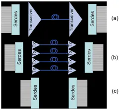
Figure 1 shows the components of typical 100G systems. A Serdes serializes a signal and transmits four 25+ Gb/s differential pairs. The 25+ Gb/s electrical signals are transmitted from the Serdes to an optical transceiver. The transceiver retimes the signals and transmits optical versions on either single-mode (SM) or MM optic fibers. A second transceiver receives the optical signals, converts them to electrical, and transmits them to another Serdes for deserializing. The purely electrical version follows the same scheme without the intermediate transceiver-driven optical signaling.
Whether for transmitter or receiver testing, optical or electrical, patterns are required to test every aspect of a component or system. The pseudo-random binary sequences (PRBSn) are standardized patterns with every permutation of n bits. The OIF CID jitter tolerance pattern is designed to have the most aggressive elements of the PRBS31 plus 72-bit sequences of consecutive identical (CID) bits but at a manageable length.
All transmitter tests, both electrical and optical, should be performed with every system channel active in both directions to include all reasonable sources of crosstalk interference. To prevent unrealistic data-dependent interference, test patterns on the crosstalk channels should differ from the test signal pattern. If it’s not possible for each aggressor to transmit a unique pattern, at least introduce sufficient delay between them so that the patterns aren’t synchronized.
Crosstalk channels also should operate with asynchronous timing for a couple of reasons: first, except in special cases, each channel operates with a clock that has been independently recovered from its incoming data. While each clock operates at the same nominal rate, they are neither frequency locked nor phase locked. Second, synchronous crosstalk has different properties than asynchronous crosstalk. Synchronous crosstalk degradation occurs in the same region of the test signal eye diagram every time an aggressor makes a logic transition. Asynchronous crosstalk, on the other hand, causes randomly timed degradation.
Stressed receiver tolerance tests are designed to assure that every compliant receiver can operate at the specified BER even with the worst-case compliant input signal. For 100 GbE IEEE 802.3ba and Fibre Channel 32GFC, the specified BER is 10-12; for OIF-CEI, it is 10-15.
Testing Optical Transmitters
Eye mask tests can be performed on either a low-noise equivalent time sampling oscilloscope or a bit error rate tester (BERT). In both cases, wide bandwidth optical-to-electrical receivers and clock recovery units are necessary. The clock recovery -3 dB bandwidth differs among specifications, typically BW = fdata/1667. The optical-to-electrical receiver should apply a fourth-order Bessel-Thompson filter with a reference frequency of three-fourths the data rate, fref = ¾ fdata. The filter is required to ensure that different test platforms can operate under uniform measurement conditions.
The random nature of a mask test is addressed by requiring a minimum hit ratio. The hit ratio is defined as the ratio of the number of mask violations to the total number of samples acquired per unit interval. Since this is a statistical measurement, the more hits, the greater the accuracy. A transmitter is compliant if it achieves a hit ratio less than 5×10⁻⁵.
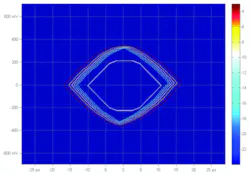
Alternatively, it’s both more statistically reliable and easier to measure the BER contour with an instrument like a sampling oscilloscope or BERT that deploys jitter and noise analysis software. As long as the BER = 10-6 contour is outside the mask as shown in Figure 2, the transmitter passes the 5×10⁻⁵ hit ratio eye test. The BER contour technique also makes it easier to see the passing margin.
The BER = 10-6 contour, the outer yellow-orange contour, corresponds to a 5×10⁻⁵ hit ratio.
Testing Optical Receivers
The optical receiver stress tests for the long- and extended-reach 4×25 Gb/s topologies (100GBASE-LR4 and 100GBASE-ER4) are similar except that greater sensitivity and robustness are required of ER4, as indicated in Table 2. At these data rates, a key challenge is producing compliant stress levels. With the appropriate options, a BERT can be used to generate a conformant, stressed eye using its internal impairment system for driving a tunable laser-based signal into the optical receiver device under test.
The sum of effects from all stressors is prescribed to meet the vertical eye closure and J2 and J9 jitter specifications.
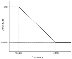
Typically, this involves configuring the BERT to drive a Mach-Zehnder (MZ) optical modulator (OMA). Then tune the MZ bias to optimize 1/0 symmetry, but don’t exceed the optical modulation amplitude, as noted in Table 2. Next, sinusoidal jitter (SJ) is applied to the pattern generator clock according to the template in Figure 3 to assure that the receiver can track low-frequency jitter.
Following this, Inter-Symbol Interference (ISI) is generated with a 4th order Bessel-Thompson filter. As specified by the IEEE 802.3ba stress-conditioning block, this 19-GHz low-pass filter characteristic removes higher order harmonics from the test generator output to permit a more consistent approach to measuring the vertical eye closure penalty and data dependent jitter (DDJ).
RJ is applied using a precision Gaussian noise generator. Gaussian RJ can be imposed on a signal by adding the noise and then subjecting the signal to a limiting amplifier. For the precision required at these data rates, the AM-to-PM conversion of a limiter is an ideal method for applying RJ.
Though not yet required in any released standards, expect to see random noise (RN) required in specifications as the industry gains more experience at 25+ Gb/s. RN also can be introduced by adding precision Gaussian noise to the signal but without a limiter.
Setting the vertical eye closure penalty (VECP) to the level in Table 2 is a multistep process. Optical VEC is given by
where the eye height, EH(2.5×10⁻³), is the vertical eye opening defined at a BER. While conceptually cumbersome, EH(BER) is a more precise definition than average peak-to-peak voltage swing. It is equivalent to the vertical distance at the center of the eye between BER contours of 2.5×10⁻³.
After setting VECP, the next step is to tune the J2 and J9 jitter levels, which indicate the properties of the jitter distribution. The high probability jitter, 99% of the distribution, is contained in J2, hence J2 is equivalent to the total jitter (TJ) defined at BER = 2.5×10⁻³. On the other hand, J9 indicates the low probability, RJ-dominated tails of the jitter distribution, the outer billionth; hence J9 is equivalent to TJ at BER = 2.5×10⁻¹⁰. Sinusoidal interference (amplitude modulation) is added to the signal until the J2 requirement is reached.
Because of the wide BER disparity between J2 and J9, a tiny amount of rms RJ raises J9 to the required level with only a tiny effect on J2. Particular care needs to be taken to ensure the intrinsic RJ of the generator source is lower than 332 fs, otherwise a simultaneous J2 and J9 intercept becomes impossible. To add very small amounts of RJ beyond the noise floor of the instrumentation, a precision RJ noise source can be used to add femtosecond levels of RJ into the signal path.
To perform the test, the stressed signal is transmitted into a replication of the system along with three other signals for crosstalk measurement. If the receiver is capable of counting its own BER, testing can be completed. If not, connect the receiver output to the BERT instrument. If the receiver doesn’t provide a clock output, you should use a clock recovery unit to time the error detector. If you don’t have a clock recovery unit, you might be able to use the BERT clock output since the output of the receiver has been retimed and should be pristine.
Apply the stressed signal to the receiver, first with low-amplitude SJ applied above the roll-off frequency. If the receiver operates at BER ≤ 10-12, then with all other stresses applied, continue the tests across the SJ frequency-amplitude template in Figure 3. If the receiver operates at BER ≤ 10-12 for all tests, it’s compliant.
Testing Electrical Transmitters
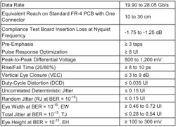
Typical electrical transmitter test requirements are shown in Table 3. Transmitter characteristics can be measured on either a sampling oscilloscope or BERT. In either case, a reference receiver is required with a golden PLL, such as a high-end clock recovery unit. Note that the transmitted signal amplitude specification is in terms of eye height EH(BER) while eye width is EW(BER).
Since electrical transmitters at these rates apply signal pre-emphasis to partially correct channel response, compliance test boards are inserted between the transmitter outputs and test equipment. Just as each specification has different requirements depending on application and length of transmission on PCB, compliance boards have different loss and frequency response profiles.
At least three taps of pre-emphasis are required. Three taps means that the voltage levels of a bit making a transition as well as those preceding and following it are modified to compensate for the channel frequency response. The tap values, C-1, C0, C1, are derived from at least eight UI of the channel pulse response. Think of the ISI introduced by the channel as the effect of folding the channel frequency response over the profile of each transmitted bit. The resulting waveform of each bit can extend over many UI. Typical 25+ Gb/s specifications require optimization over at least eight UI.
Testing the transmitter with intermediate pre-emphasis values is a good starting point. Introduce the compliance board, choose a trace that’s about the minimum prescribed length, and optimize the transmitter pre-emphasis scheme. If the resulting pre-emphasis level is less than half that allowed, use a slightly longer trace. If it’s much larger than half that allowed, try a slightly shorter trace.
Eye diagrams at these data rates, even after transmission across just a few centimeters of PCB, can be closed at the receiver, even with pre-emphasis. Accordingly, some specifications also require that the test equipment apply a continuous time linear equalization (CTLE) scheme. This way the interaction of transmitter pre-emphasis and minimal receiver equalization is included in the test. The CTLE typically is a single zero, two-pole filter that peaks at the Nyquist rate, fdata/2.
Different specifications require different test patterns. For transmitter testing, a PRBS9 pattern usually is sufficient. Of course, all other system channels should be active so that crosstalk is included in the tests. Crosstalk aggressors should transmit different patterns, and the aggressors should be asynchronous.
With the compliance board in place and pre-emphasis optimized, configure the CTLE gain as defined by the spec, typically 1 dB to 3 dB, to produce the greatest EH(BER). If you’re using an oscilloscope, collect at least 12 million samples; if you’re using a BERT, acquire at least 4 million bits. The greater the statistical sample, the better.
EH(10-15) is the vertical separation of the inner BER = 10-15 contours at the center of the eye. Similarly, EW(10-15) is the horizontal separation of the inner BER = 10-15 contours at the eye center. VEC is the ratio of the average voltage swing and eye height:
Testing Electrical Receivers
Stressed receiver tolerance testing is meant to subject the receiver to the worst-case signal. If the receiver, including its internal equalization scheme, operates at or less than the prescribed BER, BER ≤10-12 for 100 GbE and 32GFC and BER ≤ 10-15 for OIF-CEI, then the receiver is compliant.
Each specification requires different levels and types of stress. Some only require SJ. Be sure to check the specification to which you are testing to guarantee that your test is compliant.
To configure the stressed signal, connect the compliance test board between the BERT’s pattern generator output and error detector input. Then generate a PRBS31 test pattern; a long pattern with every permutation of 31 symbols to produce every imaginable bit trajectory. From there, you will need to apply other impairments such as DJ, crosstalk, sinusoidal interference, and RJ. To perform the test, assure that the receiver sees the signal you’ve configured. It’s best to connect the receiver to the compliance board with the same cable used to set up the test.
If the receiver is capable of counting its own BER, you’re ready to go. If not, connect the receiver output to the BERT error detector. If the receiver doesn’t provide a clock output, you should use a clock recovery unit to time the error detector. If you don’t have a clock recovery unit, you might be able to use the BERT data-rate clock since the output of the receiver has been retimed.
Apply the stressed signal to the receiver first with low-amplitude SJ applied above the roll-off frequency according to that shown in Figure 3. If the receiver operates at or better than the specified BER with its equalization scheme enabled and optimized, continue testing across the SJ frequency-amplitude template in Figure 3 to assure that the receiver can track low-frequency jitter with all other stresses applied. The receiver is compliant if it operates at or better than the specified BER across the SJ frequency range.
Diagnostic Tests
The difference between compliance and diagnostic tests is complexity. Compliance tests tend to include too many elements for straightforward interpretation. To determine which elements or components of a system might be causing problems, diagnostic tests should be strategically planned to probe specific weaknesses. They should build in complexity, test upon test, to find problems and determine margins.
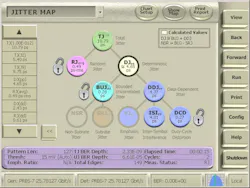
If the transmitter fails, simplify test conditions by removing any test compliance boards and analyzing the transmitter output with as direct a connection as possible. Perform jitter and noise analysis. Analyze the breakdown as you apply more complex patterns, introduce increasing lengths of PCB, apply pre-emphasis, and turn on crosstalk aggressors. For each set of conditions, analyze eye diagrams, BER eye, BER contours, and the jitter and noise breakdown as shown in Figure 4.
Similarly, when the receiver fails, you will need to investigate the receiver’s response to each stress. Use the features of the BERT’s pattern generator function. Start with a clean pattern and add complexity.
- Apply test patterns with low mark density to check for baseline wander.
- Challenge clock recovery circuits with patterns that have long strings of CID bits and low transition density. The more structure a pattern has, the more ISI it generates when applied to a compliance board or filter.
- Sweep SJ across the receiver’s clock recovery frequency response at different amplitudes. Determine where the clock recovery circuit’s capability to track jitter breaks down.
- Challenge the receiver’s equalizer by introducing increasing lengths of compliance board. By combining pattern complexity and trace length, you can generate a wide variety of ISI levels and find an equalizer’s margin.
- Probe the receiver’s capability to tolerate jitter and noise; that is, its setup and hold, by ramping up BUJ-crosstalk and RJ.
- Check the voltage sensitivity by introducing sinusoidal interference.
Find the sensitive aspects of the receiver and then apply different stress combinations. There may be stress combinations that are particularly challenging as well as peculiar combinations where the receiver is quite robust.
Summary
Signal transmission at 100 Gb/s is not simple, and many of the standards are still evolving. At 25+ Gb/s transmissions speed, the jitter budget has all but disappeared, and the industry is still building experience around transmitter and receiver testing at these speeds. Therefore, it is vital that engineers building 100G systems have a solid understanding of how analog waveforms relate to digital signal BERs and ensure they are measuring with test instrumentation featuring low intrinsic jitter and noise to maximize jitter budgets.
Acknowledgement
This article is adapted from Physical Layer Tests of 100 Gb/s Communications Systems, a Tektronix application note, 2012.
About the Author
Chris Loberg is a senior technical marketing manager at Tektronix. He has held various positions with Tektronix during his more than 13 years with the company, including marketing manager for the Optical Business Unit. Previously, he was employed by Grass Valley Group and IBM. Loberg earned an M.B.A. in marketing from San Jose State University. [email protected]
About the Author
Voice Your Opinion!
To join the conversation, and become an exclusive member of Electronic Design, create an account today!

Leaders relevant to this article:


