Systems and software address testability
Printed-circuit-boards present significant test-and-measurement challenges as complexity and performance increase and components shrink. Traditional in-circuit testers and flying probers have a role to play, as do automated optical and X-ray inspection, but techniques based on boundary scan are increasingly playing a complementary role. Further, test technology engineers are extending boundary-scan derived techniques not only to look beneath LGAs and BGAs but to peer deep inside board-mounted chips. Ultimately, the domain of the circuit-board engineer extends from design capture to production test.
Over the past year since IPC Apex Expo 2015, “Our interactions with customers are all pointing to a greater need for solutions to help reduce their scrap piles from mobile boards to all sorts of sensor boards,” said NK Chari, director of marketing and support at Keysight Technologies’ Measurement Systems Division. “The key here is to take a deeper dive, going beyond the standard board and functional test for the PCBAs and trying to better understand our customers’ problems.” Keysight’s key differentiator, he said is to “… improve product quality right from the design-for-test phase while reducing the cost of test.”
Key drivers are loss of test access and increasingly faster and higher-powered components. “For example, in 2015 we saw the adoption of DDR4 and LPDDR4 pick up significantly, and there was a concurrent need to ensure good test coverage,” Chari said. “HDMI boards were another area of interest, which caused us to further push the test capabilities of our x1149 boundary-scan analyzer. Moving forward, the need for more of such embedded test capabilities will grow as the industry continues to take up even newer technology for NAND flash, embedded multimedia controllers, multicore processors, etc.” The company’s boundary-scan team, he said, is working on test applications from the initial DFT stage to volume production.
There still is an important role for traditional board test, Chari said, “But it’s a matter of moving beyond the comfort zone with a solution. For a long time, our i3070 and i1000 in-circuit test (ICT) solutions have become a de rigueur part of quality control. But customers also want them faster, leaner, meaner.” When Keysight introduced the fully automated i3070 and i1000 inline in-circuit testers, he said, people were curious but hesitant to adopt automation. “We know human nature is somewhat resistant to change,” Chari said. “However, we are very glad to observe that since last Apex, receptivity to our inline ICT solutions is really taking off as end users start adopting them much more readily.”
Keysight now is ready to roll out phase 2 of the ICT automation process. “We are continuing to shrink the footprint of our testers while offering better usability, such as new features on the latest 09.00 software and improved test coverage,” Chari said.
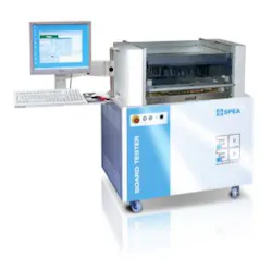
GOEPEL electronic also sees a key role for boundary scan and has announced the availability of boundary-scan integration into SPEA’s multicore ICT platform. With the level of integration provided for the SPEA 3030 ICT system, execution of interactive boundary-scan tests now is possible on all cores of the ICT (up to four), GOEPEL said, adding that simultaneous execution of different test sequences opens up technological and economic advantages supporting the parallel test of several UUTs.
Courtesy of SPEA
The boundary-scan integration option from GOEPEL has been available in selected SPEA ICT systems for several years, GOEPEL said. The new integration enables real parallel test execution involving all resources of the SPEA 3030 ICT system (Figure 1). The SPEA LEONARDO software initializes the tests of the GOEPEL CASCON boundary-scan software, which is able to activate measurement and driver instruments of the ICT system—thereby achieving a real interaction between boundary scan and the individual ICT cores. CASCON then transfers the test results to the SPEA software and assigns them to the respective cores.
Evolving boundary scan
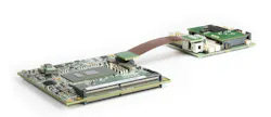
GOEPEL also has been working to evolve its boundary-scan technology beyond the board and into the chip. One result of this effort is the recent announcement that the company’s VarioTAP model libraries now support the sixth-generation Intel Core processors, codenamed Skylake, whose BGA and LGA packaging typically prevents direct contact with external instruments. VarioTAP models allow flexible execution of processor emulation tests using the processor’s native debug interface, offering embedded instruments for test, hardware debug, and design validation even after mounting. This enables users to accelerate prototyping, shorten time frames for new product introduction, and ensure the quality of production test with reduced access. GOEPEL realized the development and verification of the VarioTAP models in cooperation with Congatec, using the conga-TC170 fanless, sealed COM Express module (Figure 2).
Courtesy of GOEPEL electronic
Also addressing boundary-scan technology with new initiatives is ASSET InterTech. The company’s HSIO (high-speed input/output) Validation Assistant (HVA) is a new datamining tool for ASSET’s ScanWorks boundary-scan platform. HVA automatically analyzes a database of signal-integrity test data and quantifies the risk associated with potential design flaws or poorly performing devices on a system’s HSIO buses.
As the throughput on HSIO buses has increased, they have become more sensitive to interference, and their operating margins relative to their eye masks have decreased. The slightest design or assembly flaw or a variation in the components on the circuit board can severely reduce HSIO throughput, possibly causing a system crash, according to Tim Caffee, ASSET’s vice president of design validation and test. Many silicon providers, including Intel, have recommended an extensive battery of validation tests on all of the lanes on the SerDes HSIO buses on system circuit boards. And, these tests typically are performed on multiple prototype circuit boards. A simple pass/fail test, Caffee said, would not show how close the bus signaling is to its eye mask. By knowing the operating margin and analyzing it statistically, engineers can associate a level of confidence with the system’s operations.
ScanWorks HVA automatically organizes and correlates the validation database gathered by various validation teams in an organization so engineers can efficiently identify vulnerabilities. In addition, redundant validation testing can be identified and eliminated to speed up the validation process over the life cycle of the product.
“Continually validating a system over all of its life cycle has become tremendously important and much more complicated as the speeds of HSIO buses have escalated,” said Caffee. “For example, Intel might recommend that the HSIO on a design should be validated with a suite of five tests on five different prototypes. Statistically analyzing all of that test data is not straightforward, so, unfortunately some system suppliers still rely on pass/fail validation testing, and that is inadequate if you want to project the risks associated with a design. HSIO Validation Assistant gives engineers the information they need in a view that makes the most sense to them.”
ScanWorks HVA has been integrated into the ScanWorks HSIO tool that validates the signal integrity on all of the high-speed buses on Intel circuit board designs, including QuickPath interconnect, serial management interface, double data rate memory bus, PCI Express, PCIe Graphics, direct memory interface, serial ATA, and universal serial bus.
Beginning with design
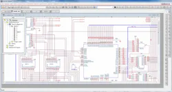
PCB designs typically begin with schematic capture, using software like Cadence OrCAD Capture. “OrCAD Capture is the de facto industry-standard schematic capture product in the business,” said Manny Marcano, president and CEO of EMA Design Automation, a full-service provider of EDA tools. In January, EMA announced a North American OrCAD Capture maintenance (Figure 3) initiative aimed at delivering technology to IoT innovators and the maker community. “In today’s economy, there are many innovators in large and small companies that want to bring their ideas to life as products but might not have the budget for the best tools,” said Marcano in a press release. “We want to fix this situation.”
Figure 3. Cadence OrCAD Capture screenshot
Courtesy of EMA Design Automation
Typically, throughout the EDA industry, the initial purchase of any product includes software cost and a one-year maintenance cost. To address the needs of the innovator, EMA is offering Cadence OrCAD Capture for only the cost of maintenance. The benefits are product updates and bug fixes for a year, live phone support by EMA’s technical team, access to the EMA resource center, and access to Cadence online support.
EMA also offers a three-month license of OrCAD Library Builder, enabling an engineer to quickly create symbols, footprints, and 3D models for numerous part types. Tutorials and a self-paced training course lead new users through the software to get them proficient with OrCAD Capture quickly.
“At the end of the maintenance period, customers can choose whether to pay for another year of maintenance. Whether they do or not, the software is theirs,” added Marcano. “We find that the vast majority of OrCAD customers choose maintenance each year so they can benefit from product updates and support.”
A key aspect of PCB design is ensuring testability. To that end, Aster Technologies offers the TestWay electrical DFT analyzer, which enables validation of designs at the schematic-capture stage to ensure that adequate measures have been included to comply with the manufacturer’s test requirements. The ability to verify that PCB designs have been developed with adequate design-for-test in mind, the company says, is key in determining the most effective test strategies and accurately calculating fault coverage, which are crucial in improving competitive advantage, lowering cost, and ensuring product quality.
Complementing electrical test
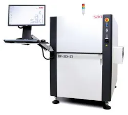
Courtesy of Saki
Electrical test techniques extend from prototype to production, but optical and X-ray inspection can add valuable information in production. Addressing this area, Saki, a provider of automated optical inspection (AOI) equipment, debuted its third-generation 3D AOI line, offering throughput increases of 15%, at NEPCON Japan Jan. 13-15 in Tokyo. Saki’s new BF-3Di-D (dual-lane) and BF-3Di-Z (extra large platform) 3D AOI equipment (Figure 4) provides measurements of components with a height range between 0 and 20 mm, achieving 1-μm height resolution, a false call rate of less than 100 ppm with zero escapes, and an increased positioning speed of 50%. The new camera and lighting systems capture clear, detailed images with no shadowing for inspection of the most difficult defects, such as lifted leads, tombstones, reverses, and height variations.
Saki also demonstrated its 3D automated X-ray inspection system that provides 100% head-in-pillow detection. This system takes up to 200 slices of a component and inspects and measures the solder-joint structures, with on-the-fly reconstruction and volume measurements, creating 3D data for the entire sample. The system perfectly separates the top and bottom sides of the PCB for extremely high-resolution images and best-in-class process capability and gage repeatability and reproducibility, which are especially needed for applications in the aerospace, medical, and automotive markets where reliability is critical.
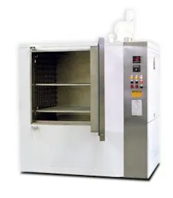
And finally, once your board is tested and inspected, you may want to protect it. For that purpose, Grieve offers a class 100 cleanroom cabinet oven—dubbed No. 797 (Figure 5). The 260°F (127°C) electrically heated oven currently is used for drying coatings onto PCBs at the customer’s facility. Workspace dimensions of this 20-kW oven measure 36” W x 36” D x 39” H. A 1,000-cfm, 1.5-hp recirculating blower provides horizontal airflow to the workload.
Courtesy of Grieve
The oven features 4-inch insulated walls, a stainless steel interior with continuously back-welded seams, an exterior finished with white epoxy paint, a brushed stainless steel door cover and control panel face, a 30” x 24” x 6” thick stainless steel high-temperature HEPA recirculating filter and all safety equipment for handling flammable solvents. Controls on No. 797 include a digital-indicating programming temperature controller and an SCR power controller.
Apex Expo 2016
At Apex 2016 March 15-17 in Las Vegas, Keysight will highlight a new solution to improve the efficiency of test development and debug of boundary-scan tests for multiple boards with long chains, and it will present a solution that aims at improving test coverage of server boards using test cards. “All these will be enabled on our power-packed x1149 boundary scan analyzer,” Chari said. “The form factor is just slightly larger than our palm, but we are pleased to push its boundaries even further with these new applications.”
He added that contract electronics manufacturers and specialized automotive electronics manufacturers that desire automation and space maximization can look forward to the latest i3070 in-circuit test solutions—a lean inline solution as well as offline solution with a robotic arm. Both solutions are helping users to automate board-test processes and reduce footprint. “We have spent a fair amount of effort to make ICT automation state of the art,” Chari said, in order “… to pack more punch per inch of the system …” to maximize the line capacity while simultaneously optimizing human resources, enabling people to be redeployed, leaving the board test routines to the machines.
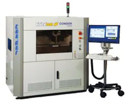
Digitaltest said it will show its new Condor MTS 505 (Figure 6) flying-probe system and Digitizer 2.0 reverse engineering software. The Condor flying-probe solution provides larger board capability, faster programming, and increased optical capability for low- to medium-volume production. The new Digitizer 2.0 helps recover CAD data. Digitizer generates a CAD file for the board that contains all the board components and nets. The file can be used for board test, repair, and/or remanufacture.
Courtesy of Digitaltest
Also at Apex, JTAG Technologies will showcase its JT 5705 Series boundary-scan controller hardware for PCB assembly and system testing. The series incorporates both JTAG/boundary-scan controller functions and mixed-signal I/O channels. The first in the series—the JT 5705/USB—is supplied as a desktop instrument, primarily aimed at hardware validation applications in design, small-scale production test, and in some cases, field service and repair. The second model is the larger JT 5705/RMI, a 1U-high 19-inch rack-mountable instrument for use in systems or as a benchtop tester.
JTAG also said it will be touting the motto “Optimize your ATE with JTAG Technologies Inside.” At Apex, the company will explain that ICT, MDA, or flying-probe systems can be upgraded with JTAG Technologies’ boundary-scan solutions via special add-on cards and software integration suites that enable users to benefit from the features of the combined systems.
Peter van den Eijnden, managing director of JTAG Technologies commented, “We are cooperating with renowned ATE suppliers to make sure that our customers will continue to enjoy optimal use of their existing ICT/MDA/FPT/FCT systems throughout the coming years. In joint efforts with various test system manufacturers, we developed special hardware and software solutions. These special solutions enable perfect integration of our tools into these test systems so users benefit from advantages of the combination of both methods.”
For more information
About the Author
Voice Your Opinion!
To join the conversation, and become an exclusive member of Electronic Design, create an account today!

Leaders relevant to this article:
