Most real-world variables are analog—the speed you’re traveling, your car’s tire air pressure and its battery voltage. These and many other quantities are being monitored by millions of sensors—soon to be several billions as the Internet of Things gains momentum.
Sensors typically produce analog outputs proportional to the variable being sensed, which means that conversion to digital format is required before signal processing computer algorithms can be applied. Alternatively, analog signal processing offers many advantages, especially for low-power applications.
From at least the 1980s, a number of groups have developed field programmable analog arrays (FPAAs) but with little commercial success. Most of the research was done at institutions such as Georgia Tech, the University of Toronto, and West Virginia University, and a few semiconductor companies also became involved.
The common goal of all the groups has been to simplify the custom analog design that often is necessary to deal with a particular type of sensor. FPAAs are ideal for relatively low-frequency prototypes and research. However, FPAAs may not be the most cost-effective large-scale production solution.
A 2013 Planet Analog article includes an FPAA timeline from 1988 to 2000, which lists Pilkington Microelectronics, International Microelectronic Products (IMP, today Dialog Semiconductor in Europe), Zetex Semiconductors, Motorola, and Lattice Semiconductor. In the article, Scott Elder, the author, comments, “… FPAAs will never come to pass…. You would think that after nearly 30 years of trying, someone would have figured it out by now if it were possible.”1
In fact, two small companies claim to have succeeded: Anadigm and Aspinity. As the company’s website states, “Anadigm is the inventor, pioneer, and world’s leading supplier of dynamically programmable analog signal processors. The company was formed in 2000 with the support of Motorola and leading venture capitalists as a fabless semiconductor company.” According to Elder, Anadigm’s lineage begins with Pilkington, Motorola having purchased rights to the technology in 1997, only to withdraw from the market the following year.
An article by Aspinity’s co-founder and president Brandon Rumberg notes, the company “… develops high-performance sensor system ICs based on its analog processing technology.”2 At present, this is in the form of the reconfigurable analog/mixed-signal platform (RAMP) IC and associated software. The company’s website adds, “Aspinity’s innovations enable data to be processed at the sensor in the native analog form. By extracting application-relevant characteristics (and even meaning) prior to digitizing the sensor data, Aspinity moves data analytics to the front of the signal chain. Examples include activation of a digital speech recognizer using a high-accuracy analog voice detector or analog analysis of vibrational modes for industrial equipment monitoring. In all of these examples, Aspinity’s efficient pre-digital data analytics reduce the overall power and cost that are required.”
Under the hood
Courtesy of Georgia Institute of Technology
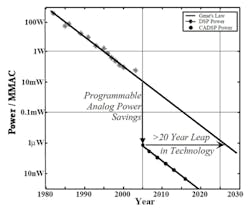
The big advantage claimed by analog processing is low power—really low. As extrapolated in a 2004 Georgia Tech doctorial thesis and shown in Figure 1,3 the power reduction achieved through analog processing would take digital signal processing 20 years to equal. Along the vertical axis, the units are power per million multiply-accumulate operations. Gene’s Law refers to comments made by Texas Instruments’ Gene Frantz, an early DSP developer. Where Moore’s law states that IC performance would double every 18 months, Frantz adds that power dissipation would decrease at about the same rate—it would halve every 18 months.
According to Aspinity’s Rumberg, in addition to being low-power, “… analog processing is able to operate in real time and inherently perform many computations that require significant overhead in the digital domain (e.g., multiplication and other nonlinear functions).”2 So, there are many reasons to consider using an FPAA for sensor signal conditioning and processing.
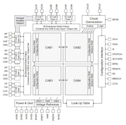
Structurally, the Anadigm AN231E04 device is easy to understand. As shown in Figure 2, it consists of a 2×2 array of configurable analog blocks (CABs) surrounded by a number of auxiliary circuits. Typical of all FPAAs, there are lots of switches to enable almost unlimited combinations of connections between parts of an individual CAB, between CABs, and between CABs and IO cells.
Courtesy of Anadigm
The word switches can mean a simple on/off function or something more complicated. Some devices have used operational transconductance amplifiers or floating gate MOSFETs as switches. In both cases, a signal can be switched from input to output but additional analog effects also can be accomplished beyond a simple on/off state.
Each of Anadigm’s CABs is programmed by data stored in an associated SRAM. A shadow SRAM allows a different configuration file to be stored without interfering with the present operation. Quickly switching to the shadow SRAM implements the device’s dynamic reconfigurability. In addition, as the datasheet states, “The AN231E04 device features seven configurable input/output structures: Each can be used as input or output; four of the seven have integrated differential amplifiers. There is also a single chopper-stabilized amplifier that can be used by three of the seven output cells.”
The user manual for the device further states, “Signal processing is accomplished using an architecture based on switched capacitor circuit design. Every CAB contains two op amps, a comparator, banks of programmable capacitors, and a collection of configurable routing and clock resources. With switched capacitor signal processing, the absolute value of the components integrated into the chip is not important, but rather it is the ratio of the programmable capacitors employed and the clock frequencies that determine circuit response, both of which are well controlled. In order to further improve signal fidelity, all signal processing within the CABs is fully differential.”
You use the FPAA by mapping your application’s analog circuitry onto the auxiliary structures and the four CABs. This is done through AnadigmDesigner 2 software that customizes the configurable analog modules supported by each CAB. An application note lists the available functions: gain, rectification, filtering, summation, differentiation, integration, multiplication, transfer function, comparator, sample and hold, oscillator sine, and voltage (±3 VDC).
In contrast, Aspinity’s RAMP FPAA has both more and simpler CABs—here meaning computational rather than configurable analog blocks. In addition, configurable logic blocks (CLBs) also are included. A total of 20,380 switches supports both intra- and inter-CAB/CLB communication. Table 1 lists the numbers and types
of available functions in both the CABs and CLBs: BPF = bandpass filter, LPF = low-pass filter, S/H = sample and hold, LUT = lookup table.
Courtesy of Aspinity
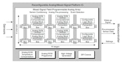
A total of 80 CABs and CLBs is arranged in eight channels, each 10 blocks deep as shown in Figure 3. According to a paper that describes the RAMP IC, “Many analog signal-processing algorithms leverage parallel signal flows to achieve efficient computation…. The CABs/CLBs in each stage are designed for specific functions, and all eight channels are identical.”4
Courtesy of Aspinity
Functionally, the blocks can be grouped in five categories:
- spectral analysis: filters, envelope detectors;
- transconductors: linear and nonlinear elements for synthesizing amplifiers, discriminant functions, and filters;
- sensor interfacing: op amps and resistors;
- transistors: to synthesize specialized computational elements; and
- mixed-signal: comparators, sample/hold, pulse generators.
The emphasis in the paper clearly is on power dissipation. Floating-gate MOSFETS provide nonvolatile analog storage for bias signals, and these values as well as the many digital settings are input via an SPI interface. While switched-capacitor technology is fundamental to the Anadigm FPAA, no mention of it is made in Reference 4 describing the RAMP IC.
Other approaches
Balanced “A” and “D”
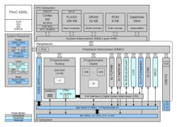
The Cypress Semiconductor PSoC 4000 Series devices have a varying complement of analog and digital capabilities depending on the model. A block diagram of the highest performing Model 4200L is shown in Figure 4, and the heavy digital weighting is easily seen. Nevertheless, with four op amps, two comparators, a 12-bit ADC, eight timer-counter PWMs, and circuitry to deal with up to 96 capacitive sensors, analog requirements have not been forgotten.
Figure 4. PSoC 4200L block diagram
Courtesy of Cypress Semiconductors
An application note5 emphasizes the device’s interconnect structure and programmability that set it apart from more constrained architectures that rely totally on the embedded CPU for control of all the peripherals. PSoC ICs instead have three separate subsystems—digital including programmable logic, an ARM microprocessor, and the analog section. Inputs to and outputs from both the digital and analog sections are independent of the CPU.
The lower performance 4000 Series devices do not have op amps or programmable logic and generally have reduced numbers of the other analog functions. These ICs also do not share the extremely low-power modes of the 4200 Series parts, which hibernate at 150 nA and deep sleep at 1.3 µA.
A series of PowerPSoC devices also is available, intended for lighting applications such as driving high-brightness LEDs. The mix of features includes up to four hysteretic mode controllers with internal 1-A MOSFETs and is capable of driving external high-power MOSFETs if higher power is required.
Microsemi has combined FPGA, CPU, and programmable analog capabilities into the SmartFusion SoC FPGA product line. Moving up from the lowest performance A2F060 to the A2F200 and A2F500 models increases the number of analog elements as well as the size of the FPGA and Flash and SRAM memories. However, most of the analog circuitry supports DACs, ADCs, and comparators. In addition, there are from one to five signal conditioning blocks with temperature, current, and voltage monitoring functions. Flash memory ensures that the chip configuration can be loaded internally at power-on.
Because of the wide range of applications that can be addressed, the SmartFusion device literature emphasizes performance aspects beyond the usual metrics. For example, under the heading Medical Systems, industry-standard security is mentioned that protects against counterfeiting and reverse engineering. Reliability is discussed as well, both in terms of the decades-long lifespan of
Microsemi cSoCs and FPGAs as well as the immunity of SmartFusion devices to “… neutron-induced configuration loss from single-event errors.”
More “D” than “A”
Lattice Semiconductor’s iCE40 LP family of ultra-low-power FPGAs is available in several sizes ranging from a 3×3-mm BGA with 25 I/O pins to a 7×7-mm 225-ball chip-scale package with 178 I/O pins. For the smaller ICs, when filled with 16-bit binary counters, the typical current drain at 1.2 V VCC and 32-kHz clock rate is about 40 µA. The devices have been proposed as very practical solutions to the interfacing problems designers face as more and more sensors are added to small platforms such as cell phones.
Although there is no separate analog section, the differential LVDS I/O buffers can be used as comparators and with some additional logic can form ADCs and DACs. An application note6 describes the common-mode range constraints on the buffers and gives a few examples of their use. In general, external resistors are needed in conjunction with the appropriately programmed internal connections to implement analog functions. Nevertheless, if you needed to interface to several sensors of different types and perform basic signal conditioning, the iCE40 devices could be helpful.
An aspect of analog signal conditioning that Aspinity’s Rumberg discusses in Reference 2 and that Lattice literature highlights is the power reduction made possible later on in the signal processing chain. For example, Rumberg cites the advantages of using analog techniques to monitor a voice channel for the presence of speech. Until an interrupt was generated by the circuitry, digital processing stages could remain in sleep mode. In contrast, traditional digital signal processing circuitry would remain turned on, first digitizing the signal and then monitoring the output for activity.
DAQ-oriented
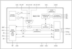
Maxim Integrated’s MAX11300 (SPI) and MAX11301 (I2C) PIXI devices shown in Figure 5 integrate a 12-bit ADC, a 12-bit DAC, associated references, and 20 fully programmable I/O pins along with a digital logic core. The serial interface is used to configure the IC. For example, the ADC can be used in a single-ended or differential mode. In addition, the I/O pins can handle digital signals referenced to a threshold set by the DAC output. This means that a wide range of logic families can be accommodated.
Courtesy of Maxim Integrated Products
Although several channels can be established, there is one ADC that is switched among the inputs. So, throughput is aggregate: It reduces per channel depending on the number of channels used. The same restriction applies to the DAC output that is switched by a dedicated sequencer block. With the serial bus in idle mode, the maximum device current is 2 µA. However, with all ports either in ADC or DAC mode, the typical current is about 17 mA. The device comes in a 6×6-mm 40-pin TQFN or a 7×7-mm 48-pin TQFS package.
The Analog Devices ADUC848 range of analog microcontrollers provides similar functionality for up to 10 channels with a 16-bit sigma-delta ADC, a 12-bit DAC, and an 8052 MCU core together with various memories and associated logic and I/O. An important distinction is the inclusion of Flash program and data memories, which means that the device does not require external configuration at power-on. The IC is available in a 52-lead 14×14-mm MQFP package for applications up to 125°C or a 56-lead 8×8-mm LFCSP package up to 85°C.
Very big “D”, little “A”
Xilinx also offers mixed-signal solutions in the company’s Artix-7, Kintex-7, and Virtex-7 FPGA families and the Zynq-7000 extensible processing platform. The analog subsystem in the -7 series parts consists of two 12-bit ADCs and a 17-channel multiplexing front end. The company calls the analog capability XADC and describes the combination of it with the FPGA logic as “agile mixed-signal.”
The ADCs in these devices run at a 1-MHz rate and use a switched capacitor input. One advantage of this architecture is that it allows the ADC’s acquisition and conversion time periods to overlap. Acquisition is allowed 750 ns, which reduce constraints on the output impedance of circuitry driving the ADC inputs. Nevertheless, anti-aliasing filters and other circuitry such as would be necessary for bridge applications must be provided external to the XADC capabilities.
Including ADCs and several selectable analog inputs makes the -7 Series and Zynq parts suitable for sensor interfacing and subsequent signal processing. However, the large amount of digital circuitry—including an ARM microprocessor in the Zynq products—does not qualify these Xilinx devices as particularly low-power solutions. Nevertheless, a diagram on the company’s website highlights the significant power reduction resulting from the 28-nm process these devices use compared to an earlier 40-nm technology.
Finding the best overall solution
Integrated interfaces for sensors are available with mixed-signal capabilities ranging from mainly analog to almost entirely digital. Very low power dissipation distinguishes a few devices, and as you might assume, these tend to be smaller both electrically and physically. Aspinity and Anadigm emphasize analog processing and low power, which set them apart from most of the other vendors.
The larger Cypress PSoC devices have a few uncommitted op amps and comparators in addition to an ADC and current-output DACs. These ICs are in the Balanced “A” and “D” subsection of this article to distinguish them from many products with ADC and DAC functionality, which is useful in DAQ applications but doesn’t support more general analog signal processing. Microsemi’s SmartFusion ICs have a number of analog signal conditioning blocks (SCBs) that contain voltage and current monitors as well as a couple of comparators. The SCBs afford a degree of analog signal processing ahead of the built-in ADCs and DACs.
Under the More “D” than “A” subsection in this article, Lattice describes the iCE40 products as being either low density or ultra low density to highlight compact packaging as well as circuitry. However, the LVDS input buffers are the only analog elements, and these can be used as comparators. The major benefits of the Lattice parts are their very low power and compact size.
Maxim and Analog Devices have developed small, comprehensive front-end circuits for DAQ applications. If you need to provide special signal conditioning, such as for a bridge-type transducer, it has to be done external to the devices.
At the other extreme of size, the Xilinx Zynq products can have very large FPGA sections together with an integrated ARM microprocessor. Obviously, these ICs address complex applications, and they also provide 17 analog inputs together with on-chip temperature and voltage monitoring via a couple of ADCs.
Which device is best for your project depends on all of these technical considerations as well as several factors not stated. For example, in some ICs, the separate analog, logic, and CPU/software skills required to most effectively configure the device may imply the need for three designers to work concurrently. A designer’s familiarity with the design tools being used to configure the new device is another important factor because learning to use new tools can add large delays to a project’s time scale.
References
- Elder, Scott, “Field Programmable Analog & Gallium Arsenide,” Planet Analog, May 2013.
- Rumberg, Dr. B., “Sensor Interface Analog Processing Improves Battery Life and Sensor Intelligence In the IoT,” Sensors Online, March 2016.
- Hall, Tyson S., Field Programmable Analog Arrays: A Floating Gate Approach, Ph.D. Dissertation, School of Electrical and Computer Engineering, Georgia Institute of Technology, July 12, 2004.
- Rumberg, Dr. B., et al, “RAMP: Accelerating Wireless Sensor Hardware Design With a Reconfigurable Analog/Mixed-Signal Platform,” Proceedings of the 14th International Conference on Information Processing in Sensor Networks, April 2015, pp. 48-58.
- Ranjith, M. and Nidhin, M. S., Getting Started with PSoC 4, Cypress Semiconductor, Application Note AN79953, February 2016.
- Common Analog Functions Using an iCE40 FPGA, Lattice Semiconductor, Application Note, October 2012.
For more information

