Thanks to advances in relay and semiconductor capabilities, switching systems continue to evolve. Higher performance relays are available with the same or smaller size footprint as older devices, making them attractive when greater density is appropriate.
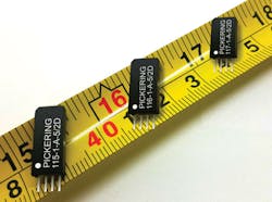
Pickering Interfaces’ Shaun Fuller, switching product manager, said, “Compared to earlier reed relay options for high-density matrix switching, the [Pickering Electronics] Series 115 reed relays (Figure 1) enabled 1-A switching … and led to a total rethink of how such solutions could be addressed. Previous designs that sandwiched two PCBs in a single module could now be achieved within a single board, not only maximizing competitiveness through dramatically reduced build costs, but also simplifying maintenance. The use of such small footprint relays also left sufficient space for configuration linking to accommodate 22 different build options and suit a large variety of user requirements. Six bus widths (x16, x12, x8, x6, x4 and x2) are available in matrix sizes comprising up to 256 crosspoints.”
Courtesy of Pickering Electronics
The company’s 40-520 range of PXI switching modules uses the type 115 relay and achieves 25-MHz bandwidth with typical -40-dB crosstalk at 1 MHz. The type 115 relay design trades height for footprint area and features integral mu-metal shielding, which allows the relays to be placed as close as possible to each other. The low crosstalk on modules that use this relay results from a small amount of coupling between relays as well as coupling between PCB traces.
Addressing trade-offs that become relevant at higher frequencies, Astronics’ Robert Waldeck, director sales/special products, discussed the need to provide sufficient relay separation in PCB layouts. He said, “Switching system design for ATE is a delicate compromise between voltage and current vs. system bandwidth as well as the overall size of the product. When one is designing for optimal bandwidth, the smaller size of the PCB works against the designer….
“In order to optimize the bandwidth,” Waldeck continued, “PCB traces need to have enough space for proper impedance and phase matching and … high-bandwidth trace routing techniques. Things like vias and sharp corners come into play as frequency increases. Stub management is also of primary importance in maintaining high performance. We have found that the arrangement of the relays and the layout of the traces on the board are more important than the selection of the switching components themselves. All of these things require significant PCB real estate to do properly.”
National Instruments uses FETs instead of relays in the Model PXI-2535/36 switches with 544 crosspoints in a single-slot 3U module. These products have the advantage of virtually unlimited life—especially important because of the high 50,000 crosspoints/s maximum scan rate. Nevertheless, among the trade-offs are 1-MHz bandwidth, 0.1-A switching current, and ±12-VDC or 8-VAC maximum voltage.
Semiconductor-based switching isn’t limited to low power. According to Pickering’s Fuller, “… depending on [the type of solid-state relay], they can also support the highest DC hot switching powers in the smallest size. However, for high-power applications, they tend to have higher resistance and worse isolation than mechanical relays.”
And, for high frequencies, NI’s PXIe-2543 solid-state dual 4:1 multiplexer is intended for use in a 50-Ω system up to 6.6 GHz. The AC-coupled switch’s insertion loss at 6.6 GHz typically is <6.1 dB, maximum <7.0 dB. Pickering Interfaces offers a similar 6-GHz SPDT solid-state switch. The Model 40-880 50-Ω switches, like NI’s PXIe-2543, can handle up to 30 dBm. The insertion loss typically is 3 dB to 6 GHz, partially because the SPDT switches are not configurable.
Neither high power nor high frequency is compatible with high density. For either the NI or Pickering module, only a small number of equivalent switch elements are involved: 16 SPDT for NI and 12 in Pickering’s 4xSPDT 40-880-002. This is a long way from the hundreds of crosspoints provided in the same size module at low frequencies. And, at microwave frequencies, bulky coaxial relays are used, which reduce circuit density even more.
Nick Turner, CEO at Cytec, said that for ATE applications, his company is concentrating on high-performance RF, microwave, high-voltage, and low-leakage solutions in which the achievable density is limited by connector styles as well as relay size. He commented that density often was a higher priority in PXI modules than in non-PXI systems.
Switching system formats
The trade-offs among numbers of channels, carry current, and bandwidth are aggravated by the small area of a 3U PXI module. And, it’s not just PCB area, as explained by Pickering’s Fuller, “In applications requiring arrays of general-purpose relays to give a more flexible switching architecture, it can be the connectors that restrict the number of relays supported, not the area occupied by the relays. This is especially true in 3U PXI due to the small front-panel size that can limit connector choices.”
Proprietary
Jon Semancik, functional/mechanical test product line manager at VTI Instruments, a unit of AMETEK, concurred with Turner and Fuller. He said, “The capability to switch higher voltages or higher currents requires larger relays and increased separation between board traces and connector I/Os. This is difficult to achieve without compromising density in small form-factor PC-based platforms such as PXI, which offer limited space to create complex architectures.”
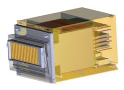
Although VTI offers a large selection of PXIe switching modules, for the most challenging applications the company chose an LXI-based approach while maintaining a modular architecture. The EX1200-SMP series uses a larger proprietary board size as shown in Figure 2 but retains the 100-mm 3U PXI board height.
Courtesy of VTI Instruments, a unit of AMETEK
To address matrix requirements, the EX1200-SMP4 four-slot carrier plugs into four slots in the EX1208 mainframe. The carrier incorporates a 16-wire analog bus that simplifies large matrix construction and maintains signal integrity by eliminating external wiring. As the EX1200-SMP4 datasheet states, “One to four carriers can be accommodated in a single mainframe with the capability to mix and match with standard EX1200 series switch cards. For example, a 176 x 8 two-wire 2-A matrix can be combined with 1.5-GHz RF mux and 16-A general-purpose relay modules to cover a wide-range of application requirements. The EX1200-SMP4 can also be configured with either resource or I/O matrix modules in any combination, which allows point-to-point I/O switching or mapping resources to UUT I/O.” Typically, system bandwidths of at least 20 MHz are achievable.
Another proprietary approach is used in the Astronics 4600 universal switching system, which was demonstrated at Autotestcon 2016. Along with several other products, the 4600 was included in Astronics’ recent acquisition of the Ascor switching product line from Giga-tronics. The term “universal switching” refers to the approach’s flexibility and is not in any way related to the company Universal Switching.
As a joint Giga-tronics and Rockwell Collins paper1 explains, this type of switching system previously had been implemented by “… some of the large system manufacturers in the semiconductor space….” The paper further describes the concept as an ATE transmission “… which takes the ATE resources and routes them directly to the DUT. By using a transmission, the concept of a software-defined I/O map becomes realized.”
Although the system does not conform to the AXIe standard, the partitioned AXIe backplane influenced its design. The paper states, “The AXIe platform has its backplane divided into three discrete sections, zone 1 for power, zone 2 for communication, and zone 3 which is user defined. Zone 3 is so undefined that the user can literally put anything in this location. It was decided to place an active switching module(s) in zone 3, which would allow us to create stub-less, homerun connections between any two cards in the chassis.”
The 4600 chassis (Figure 3) is 10U high compared to 12U or 13U for an AXIe chassis but with a depth similar to VXI. The resulting board area is larger than VXI and at least two times the area of 6U PXI. There are 21 slots on 0.8-inch pitch—the same pitch as used by PXI.
Courtesy of Astronics
As shown in the figure, vertical slots at the front of the chassis accept instrument cards and universal I/O pin cards. Rather than running a 16-wire bus along the backplane to make connections, four separate horizontal switching cards are used, each capable of handling four differential pairs.
The horizontal cards plug into the rear of the backplane and access all 21 slots. Each card contains sufficient switching circuitry to make four separate direct connections from any vertical card to any other. This is the way that the 4600 eliminates stubs and guarantees >200-MHz bandwidth between any two cards. As shown in the paper, signals are routed on a pair of microstrip lines with 100-Ω differential impedance or 50 Ω each if independently used for single-ended signals.
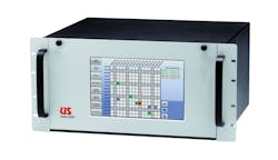
Also using a 19-inch rack-mounted chassis, but 5U high, is Universal Switching’s Model S2560F digital switching array (Figure 4). Unlike the other products in this article, the S2560F switches logical signals, not electrical ones. The output has the same logic pattern and timing as the input but has no direct, bidirectional ohmic path to it. RS-422 receivers are used on the 100-Ω inputs and RS-422 drivers on the 100-Ω outputs of this matrix with additional digital circuitry in between. The minimum size is 32 x 32, and the maximum within one chassis is 256 x 256 when all 16 I/O modules are used.
Courtesy of Universal Switching
Opposite pins on the module’s two-row 50-way SCSI-II connectors are designated signal+ and signal- so the 32 inputs and outputs can be handled as 16 differential signals. When used with a 50-Ω or 75-Ω TTL adapter panel, frequency response is from DC to 50 Mb/s and input VSWR is <1.3:1. Multiple chassis can be grouped to expand the matrix up to 1,024 x 1,024. It’s also important that the S2560F uses a three-stage full-fanout, nonblocking architecture, which means that any input can be routed to any or all outputs. This definition of nonblocking is used by many switching system manufacturers, but not all.
As described in the datasheet, “The unit comes standard with redundant hot-swap power supplies and is available with a choice of single or dual (redundant) hot-swap C3 controllers installed. The C3 controller features 10/100 Ethernet (LXI certified), USB 2.0, and multiserial (RS-232C /422A/485) control ports.”
6U PXI
The 6U format originally was included in the PXI specification as a way to ease the transition from VXI. As reported in the March 2011 edition of EE-Evaluation Engineering, “In 2007, Geotest’s [now Marvin Test Solutions] Senior Product Marketing Manager Mike Dewey said, ‘As we know now, the adoption of 6U has never matched that of the 3U form factor.’ He went on to say that Geotest had been successful partly because the 6U format existed, and in addition, both Geotest and GenRad had been more comfortable initially in adopting PXI because of the option to use either 6U or 3U.”2
As well as competing with VXI, the 6U format was a practical way to accommodate many functions that simply took more space because circuit miniaturization and integration were not at today’s levels. In the late 1990s, several influential test leaders claimed that 6U would become very popular, but it never did. Pickering Interfaces’ David Owen, in 2007 the company’s business development manager, succinctly observed, “6U PXI has apparently failed to establish dominance in the larger test market.”
Marvin Test Solutions (MTS) is one of the few ATE companies that has developed several 6U PXI modules. A larger board area allows much more design freedom than 3U PXI and is particularly important when many high-frequency channels are required as in the recently released GX6864 75-Ω RF multiplexer switch card.
As described on the company’s website, “The GX6864 provides four 2 x 16 ”… switch configurations that can be used as multiplexers or matrices. The switch card is an extended 6U PXI module with direct connection to the receiver interface.” The GX6864 achieves >500-MHz bandwidth from input switch card to RF switch card output and handles signals up to 170 V max AC peak or DC at 1 A.
According to Dewey, now MTS director of marketing, “Our … GX6864 … is designed specifically for high I/O count video-switching applications. Like other GENASYS cards, the GX6864 employs the MAC Panel 6U SCOUT receiver and offers ‘cable-less’ connection to the receiver connectors—eliminating the need for cable harnesses and the associated reliability issues that come with cabled solutions.”
Trade-offs
Several examples of currently available switching systems highlight the relationships among density and factors such as voltage and current rating, bandwidth, and signal integrity. However, as Universal Switching’s CEO Norton Alderson commented, high density is relative. He said, “Higher frequencies demand further shielding, better impedance control, and higher performance I/O connectors. For testing applications, the ideal switch needs to be as transparent as possible.”
When a switch is selected for an application, you already know that you need at least a certain number of channels; whether PXI, LXI, or a proprietary format is suitable; and the signal voltage and frequency limits. With those parameters established, a spreadsheet may be a good way to compare the remaining factors influencing your decision such as cost, relay or solid-state technology, switching and carry currents, and relevant RF/microwave characteristics if switching high-frequency signals.
In general, larger board areas promote higher density because the PCB layout is more efficient. It’s also true that a matrix usually has high density because of the repetitive PCB trace patterns that can be used, and a large-format matrix may eliminate the need for external cabling between smaller matrices. Alternatively, a large board area allows a designer to emphasize signal integrity at the expense of density by using a more conservative PCB layout and increased channel spacing to reduce crosstalk. Switching RF/microwave, high-voltage/high-current, or very low-level signals simply takes more space.
And, as Pickering’s Fuller noted, don’t forget the connectors. For example, VVK’s TEST-9110 is an AXIe-0-based cable tester with 300 independent output lines, each capable of switching 1,000 VDC at 0.5 A. In addition to the Ethernet control connectors, the front-panel area is filled by six Positronic four-row 50-pin connectors, three on each of two parallel PCBs (Figure 5). VVK is an AXIe Consortium member.
Finally, consider whether your application would benefit from a solution based on Astronics’ 4600 universal switching approach. The stub-less switched analog bus technology and the associated software-defined I/O map can be advantageous but require rethinking the instrument-switch relationship in your test system.
References
- Waldeck, R. C. and Dahl, R. W., “A Next Generation ATE Switching Solution as Applied by Rockwell Collins,” IEEE Proceedings Autotestcon 2014, p. 87.
- Lecklider, T., “PXI Matures,” EE-Evaluation Engineering, March 2011.
For more info


