Test Technique Quantifies Jitter of Discrete-Comparator Design
This file type includes high-resolution graphics and schematics when applicable.
A colleague asked for the measured jitter number on a single-supply comparator design based on the LM359 IC.1 He wanted to know how the jitter performance of the discrete comparator compared to an IC comparator, which was used with an ultrasound application.
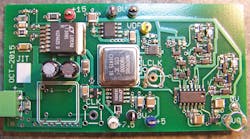
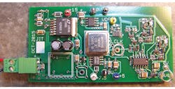
To set up the test, a special power-supply circuit was designed for the comparator as well as for a crystal-clock module with specified jitter. The power supply, clock, and comparator of the circuit (Fig. 1) were placed on a single printed circuit board (PCB) with ground plane. The board used a special scope probe-tip test point with a fitted, spiral ground wire, into which the probe’s ground-sleeve can fit. (This technique is often employed to reduce parasitic ringing and give a good return ground.) The rms jitter for this commercially available crystal-based clock module (CTS MXO45HS-3C-1M0000, 5 ps maximum) was better than the comparator could provide.
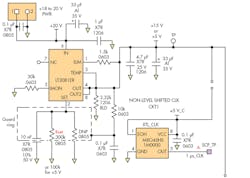
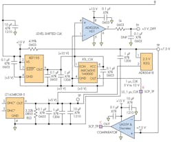
In the circuit (Fig. 2), using RSET, the main regulator (LT3081) can deliver +5 V to power either a basic clock, or +15 V to the level-shifted clock and comparator. The LT3081 was chosen as it is inherently stable with any type of load capacitance. Using this power configuration for flexibility, the non-level-shifted clock’s jitter can be measured, or the jitter of the level-shifted clock and comparator can be measured. A 5-V reference (REF195) is biased in series with a 5-V shunt reference (LT1634B-5). The crystal clock’s supply is powered with 5 V from the REF195.
The clock’s output will swing between 5 and 10 V with respect to ground. The level-shifted clock is applied to the comparator’s inverting terminal. The non-inverting comparator terminal is connected to +7.5 V, which is produced by placing another 2.5-V shunt reference (ADR5041B) in series with the 5-V shunt reference.
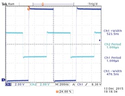
For test purposes, an instrumentation amplifier (AD8220) with unity gain is placed across the crystal clock’s power-supply pins to measure the supply’s stability during clock transitions. The integrated scope test points prevent significant overshoot and ringing on the high-speed edges of the signals from the level-shifted clock and comparator (Fig. 3).
In order to develop a test method to determine the rms jitter, a Tektronix field applications engineer recommended the “TekScope Anywhere Waveform Analysis Application” to analyze voltage-versus-time data from long record-length captures. Data captures from a Tektronix MSO4034 (a 350-MHz, 2.5-Gsample/s scope) were in their .isf format and the collected file sizes were kept to less than 20 MB, to fit email-attachment memory limits and simplify working at different locations. Both the level-shifted clock and the output of the comparator had .isf files generated by the Tektronix scope.
The signals were ac-coupled to ease scaling of the input-signal traces and make better use of the analog-to-digital converter's input range without clipping. The scope settings included sample rate of 2.50 Gsamples/s, record length of 10 Mpoints, V (clock) of 700 mV/div, V (comparator) of 1.8 V/div, time base of 100 μs/div, and ac coupling on each channel. The trigger method involved Trigger-B sequence Trigger Follow by n events, with n = 1000 events. If just an edge trigger were used, the scope triggering would try to compensate for jitter at the trigger point. (The typical jitter specification for an MDO4000 series unit, probably similar to the MSO4000 series, is less than 10 ps rms for edge-type triggers). The chosen trigger method likely reduced the effect of the instrument’s trigger jitter.
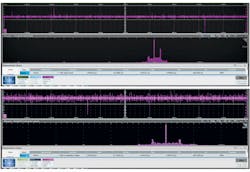
The Tektronix application was used to generate the data and plots from .isf files collected on the MSO scope, and the data was processed for standard deviation and peak-to-peak jitter. Based on the 3998 clock-period samples captured, a histogram was plotted and merged with the results from the application (Fig. 4). The upper graph is the measured period versus time, and shows that a few spikes occurred in the data at random sampling times; these will produce "outliers" in a histogram (the second graph).
The measured jitter performance of the comparator—just 23-ps rms jitter at one standard deviation with a 1-MHz input clock—exceeded design expectations. It was determined using the following equation with time in picoseconds (the jitter performance of the scope is not included):
The conclusion was that it is feasible to build a simple test PCB and collect jitter data from a high-performance circuit, if a good digital scope such as the Tektronix unit is available. The jitter results showed this comparator could work with the colleague’s ultrasound application.
Reference
1. “Dual Comparators Match Precision Industrial, Instrumentation Application Needs,” Electronic Design.
Looking for parts? Go to SourceESB.
