Reader Q&A of the Month: Alex Lidow Answers Your Questions
Power Electronics' Q&A series kicks off this month featuring Alex Lidow, CEO of Efficient Power Conversion Corporation (EPC) as the first expert to field your questions. Send us your question for Alex one of two ways: 1) use the form at the bottom of this page if you wish to post anonymously; or 2) simply post a comment in the “Discuss this Article” box below. Power Electronics will publish answers in the reader Q&A next week, so check back then! Alex’s Q&A will also appear in the PE Tech weekly newsletter, so if you’re not already a subscriber, click here to get your free subscription now. How it works: during a two week period we will collect your power industry related questions for the month's featured expert and they will *answer as many questions as possible. Responses will be published online and linked in the PE Tech newsletter.
*Our experts will answer as many questions as possible. Some questions may be fielded by other members of the expert panel.
*Our experts will answer as many questions as possible. Some questions may be fielded by other members of the expert panel.
Who is Alex Lidow?
Prior to founding EPC, Dr. Lidow was CEO of International Rectifier Corporation. A co-inventor of the HEXFET power MOSFET, Dr. Lidow holds many patents in power semiconductor technology and has authored numerous publications on related subjects. Lidow earned his Bachelor of Science degree from Caltech in 1975 and his Ph.D. from Stanford in 1977.
Below is a recent question submitted by a Power Electronics Reader, answered by Alex.Q. How do GaN transistors compare with power MOSFETs for power switching applications in terms of efficiency? Alex Lidow - To effectively compare the potential performance of a power MOSFET and an enhancement mode GaN transistor in a power conversion circuit, some figures of merit (FOM) need to be defined first. A FOM that has been used by MOSFET manufacturers to show both generational improvements and to compare their products to other competitive devices is the product of the gate charge, QG, and the RDS(ON) for a given device. What makes this so useful is that no matter the size of the die, this FOM is almost constant for a given technology or ‘Generation’ of device. This FOM is related to device performance and can be useful in predicting power loss improvements with improved technologies, but it is less sensitive to differences when a device is used more as a switching element than as a conducting element. We will therefore discuss three distinct FOMs. The first of these is the traditional FOM. We will call that the “Rectifier FOM” because it is most applicable when a FET is used as a rectifier element such as in the lower transistor of a buck converter. The second FOM we will call the “Switching FOM” because it best describes relative performance of devices used mostly as switching elements such as in the upper transistor in a classic buck converter. Of these two FOMs, the switching performance is more important in ‘hard switching’ converter circuits. The third FOM we will call the “Resonant FOM” because it best describes relative performance of devices used in resonant circuits where the switching occurs when there is zero current through the device (ZCS).
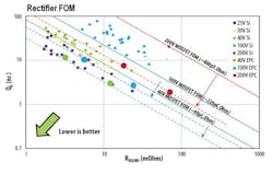
The rectifier FOM is shown in Fig. 1 and plots RDS(ON)vs. QG for the eGaN FET as well as for different equivalent silicon MOSFETs. From this we can draw a number of conclusions:40 V eGaN FETs are comparable to the best 25 V lateral silicon devices. 100 V eGaN FETs are comparable to 25 V vertical silicon devices200 V eGaN FETs are comparable to 40 V vertical silicon devices
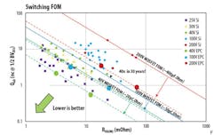
Fig. 2 plots RDS(ON) vs. QGD (Switching FOM) for eGaN FETs as well as for various equivalent silicon MOSFETs. We can see that, based on switching FOM, eGaN FETs offer a distinct advantage over any equivalent voltage rated silicon device. As with the Rectifier FOM:40 V eGaN FETs are comparable to 25 V lateral silicon devices. 100 V eGaN FETs are comparable to 40 V vertical silicon devices200 V eGaN FETs are comparable to 100 V vertical silicon devices
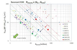
Fig. 3 plots RDS(ON) vs. QG+ QOSS (Resonant FOM) for eGaN FETs as well as for various equivalent silicon MOSFETs. When a device is switched at zero current, the major elements of switching loss come from charging and discharging the device output (QOSS) and the input gate (QG). We can see that, based on the resonant FOM, eGaN FETs again offer a distinct advantage over any equivalent voltage rated silicon device.
Whether the designer of a power conversion system is using a hard switched topology or a soft switched topology, GaN transistors can reduce the power losses and increase power density. The higher the conversion frequency, the greater the gain by upgrading to the new generation of power transistor made with a remarkable material, GaN.GlossaryParameterDescriptionRDS(ON)Drain- source on-resistanceQGTotal gate chargeQOSSOutput chargeQGDGate-to-drain chargeFOMFigure-of-meriteGaNEnhancement mode GaN transistorFiguresRectifier FOM (RDS(ON)vs. QG) for eGaN FETsSwitching FOM (RDS(ON) vs. QGD) for various eGaN FETs and MOSFETs Resonant FOM (RDS(ON) vs. QG+ QOSS) for eGaN FETsIf you would to submit your questions to Alex anonymously, please post any questions you have in the comments section below.


