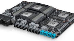
DRIVE PX Pegasus is NVIDIA’s driverless car platform (Fig. 1). The platform is designed to meet safety Level 5, self-driving car autonomy requirements as well as ISO 26262 and ASIL D functional safety specifications. The board delivers more than 320 trillion operations/s (TOPS) and is powered by a pair of Xavier system-on-chips (SoC). The Xavier incorporates the latest Volta GPU architecture designed to support deep neural networks (DNN) and machine learning.
DRIVE PX Pegasus is designed to handle up to 16 dedicated, high-speed sensor inputs. It also supports 10-Gbit Ethernet, Flexray, and CAN. It has a memory bandwidth greater than 1 Tbyte/s. Its built-in security support is designed to authenticate over-the-air (OTA) updates.
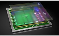
The Xavier AI system-on-chip (SoC) is designed to deliver 20 TOPS while consuming under 20 W. The CPU consists of eight 64-bit ARMv8-compatible cores. The GPU has 512 cores. There is also a Computer Vision Accelerator (CVA) and an 8K high dynamic range (HDR) visual processing (VP) unit.
The bulk of the Xavier AI SoC is taken up with the Volta GPU that has been augmented to handle AI applications—DNN in particular. The GPU alone requires more than 21 billion transistors. The GPU includes 640 Tensor Cores that deliver over 100 Teraflops/s (TFLOPS). That is five times what the NVIDIA Pascal architecture delivers.
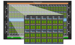
The Volta streaming multiprocessor architecture (Fig. 3) is designed to be more efficient than the previous Pascal design while boosting FP32 and FP64 performance and addressing. The hierarchy includes multiple Graphics Processing Clusters (GPC), Texture Processing Clusters (TPC), Streaming Multiprocessors (SM), and memory controllers. Overall there are six GPCs, 42 TPCs, 84 SMs, and eight 512-bit memory controllers that connect to the high bandwidth memory version 2 (HBM2).
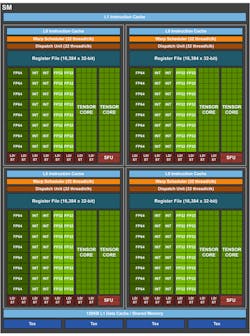
Each SM is broken into four blocks (Fig. 4) that include 64 FP32 cores, 32 FP64 cores, 64 32-bit integer cores, and eight Tensor cores. The floating point and integer cores can operate independently. Each block has up to 32 active threads.
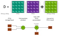
Each Tensor core provides a 4-by-4-by-4 matrix processing array (Fig. 5). The system implements a fused multiply-add (FMA) operation. Arrays A and B are FP16 while C and D may be FP16 or FP32. Each core can execute 1024 floating point operations per cycle.
Multiple Tensor cores can be combined concurrently. This allows threads to provide a larger 16-by-16-by-16 matrix operation. NVIDIA’s CUDA exposes these operations as Warp-Level Matrix Operations within the CUDA C++ API. There are C++ interfaces provided for specialized matrix load, matrix multiply and accumulate, and matrix store operations to efficiently program these cores.
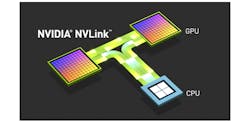
Multiple Xavier chips can be linked using Volta’s NVLink (Fig. 6). NVIDIA’s high-speed interconnect technology is designed to connect multiple CPU and GPU subsystems together.
NVIDIA now has a family of DRIVE PX platforms, including the top-end DRIVE PX Pegasus. The other platforms in the family include the DRIVE PX Xavier with a single Xavier chip, plus the DRIVE PX Parker AutoChauffeur and DRIVE PX Parker AutoCruise that use NVIDIA’s older SoCs.
