Design data formats aren’t very interesting, are they? Yes, they are. Your design data format can have a significant impact on how your company does IC design and interacts with your intellectual property (IP) suppliers and foundry. The Graphic Database System (GDS) was first introduced in 1971. Its successor, GDSII, appeared in 1978 and has been the primary IC design interchange format used ever since.
But with the sheer size of designs at the latest nodes, GDSII is struggling, overwhelmed by the demands of today’s design requirements. It’s time to move to a new “watering hole.” The challenge is deciding which alternative data format to use (through what part of your overall flow), given all the impacts of such a change through your entire design flow, and how your company interacts with your ecosystem partners.
This file type includes high resolution graphics and schematics.
What’s The Problem?
Big data means long transfer times within your company and even longer transfer times between your company and your foundry. Big data also slows down runtimes from design to physical verification, increasing the time it takes your design team to get a design to market. At 28 to 20 nm, we are seeing designs that require up to 1 billion bytes (1 Tbyte) of disk data in GDSII.
That amount of data puts us at a level of pain where it may be faster (and more reliable) to download your design to a disk drive and mail it to your foundry than to transfer it electronically. Ironically, that’s exactly what we used to do in the earliest days of IC design, although we used magnetic tapes then, instead of disk drives (the source of the term “tapeout”). How crazy is that in this day of interconnected everything and constant communication?
What’s Driving The Issue?
The historic march to follow Moore’s Law of twice as many transistors per design is clearly a key driver, but there are other influences as well, especially at 28 nm and below. Historically, the foundries minimized the amount of fill used in designs to minimize the impact on timing. But recently, they realized they can now reduce variability by maximizing fill.
Related Articles
• RTL-To-GDSII Flow Rolls For Structured ASICs
• Make The Leap From Test Chips To Production Designs At 20 nm
• Companies Ramp Up To Move From 20 nm To The Next Node
The major foundries made this change in fill strategy at 28 and 20 nm. At the same time, they transitioned from polygon-based fill to a “smart” cell-based fill technique. While this cell-based fill strategy is far more compact than if the industry continued to use a polygon-based approach, nonetheless, the changeover to fill maximization significantly increases design size above the historic trend.
Another driver is the addition, on average, of one or two back end-of-line (BEOL) wiring layers node over node. You can expect this rate to increase at an even higher rate with the adoption of double patterning/multi-patterning at 20 nm and below.
Options
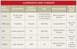
So, GDSII is the primary format used today to represent design data for IP in transfers to and from EDA tools in your design/verification flow and to your foundry. What are our options beyond GDSII? Proprietary and pseudo-proprietary alternative data formats both are currently available (see the table).
Proprietary formats are defined and controlled by one company, such as Milkyway, which is owned by Synopsys. Pseudo-proprietary formats have been donated to an industry/standards body at some point but don’t include advanced functionality developed after the donation. Pseudo-proprietary formats include the Design Exchange Format (DEF), which is owned by Cadence and managed (for the open specification) by the Silicon Integration Initiative (Si2) and OpenAccess (OA), which is owned by Si2.
Our other option is the Open Artwork System Interchange Standard (OASIS), which is owned and maintained by the trade and standards organization Semiconductor Equipment and Materials International (SEMI).
Tradeoffs In Data Format
The tradeoffs between these different options break down into three areas: flexibility, interoperability, and performance. The proprietary and pseudo-proprietary formats are effective while in custom or place-and-route (P&R) design implementation, as they can include additional meta-information such as timing and connectivity necessary for design layout. Owners of the proprietary and pseudo-proprietary formats advocate for their use, arguing that their design tools can:
• Pass design intent forward to the foundries
• Provide a common data model across your entire IP EDA flow (implementation, verification, etc.), enabling you to work more efficiently and achieve faster time-to-market
• Produce faster runtimes, etc.
Sounds good, right? No, it isn’t good. The penalties for pursuing this path are significant. First, the foundries only accept GDSII or OASIS, so there is no design intent that can be passed forward from a proprietary or pseudo-proprietary format.
Next, there is no single or common data model available within any one of the EDA vendors. Even if there were, the argument that standardizing on one data model throughout the flow gives you a better overall implementation and verification solution doesn’t hold either. No one supplier is good at everything (e.g., custom, P&R, verification, extraction, etc.). Trying to standardize on a “single” data model and supplier means you are choosing a suboptimal overall flow. Leading companies use the best-in-class tools from each vendor across at least two data models.
Third, most companies use custom and P&R tools from multiple EDA vendors. Standardize on a proprietary/pseudo-proprietary format from one vendor, and it won’t work with any of the others—clearly, interoperability will be a problem. And given that most companies change their preferred P&R or custom design tool every technology node or two, standardizing on a proprietary format means their flexibility to change is significantly curtailed.
Finally, the pseudo-proprietary formats also suffer the issue previously alluded to—when new features are needed, the source company may hold them in proprietary status, often delaying open availability by months, if not years. This has been a significant problem at the 20-nm node, with double patterning driving the need for extensions to DEF and OA that were available from the supplier controlling the format long before they were available to other EDA vendors and users across the ecosystem.
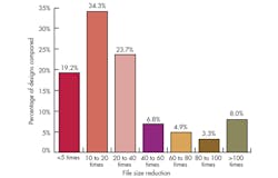
So what are the tradeoffs with OASIS? It is an open standard that can be used for IP through full chip (i.e., front end of line (FEOL) and BEOL designs). All three major EDA suppliers can read and write it reasonably well. It provides an enormous reduction in data volume (see the figure). And, OASIS capabilities in P&R and physical verification tools are mature. The larger challenge is standardizing on the use of OASIS in IP implementation and the ability of homegrown customer and second-tier EDA applications to read and write OASIS data.
A Practical Path Forward
The foundries and many advanced-node fabless companies have adopted (or are in the process of adopting) OASIS on the manufacturing side. Now is the time to make the same change on the design side. Your company’s move to 20 or 16/14 nm creates a natural opportunity to make the transition to OASIS.
To meet the foundry design rules, IP for 20 and 16/14 nm must be new. You can’t just shrink IP from the prior node. Most companies will only move one design team at a time to 20/16/14 nm. Since you are retooling your flows and IP during this jump for one design team, change the data format to OASIS at the same time. There is even a GDS2OASIS conversion utility (donated by Mentor) that is available to anyone using OASIS.
Since the greatest data size pain is felt at the back end (i.e., P&R to physical verification and tapeout to foundry), and these tools/flows are more prepared, start here. One note of caution—you want to avoid conversion to OASIS at the last minute in your flow. You want to be performing continuous physical verification in the format you will be taping out to the foundry, because errors found early are cheap and easy to fix. A last-minute conversion can lead to expensive errors (in both time and resources) that are only discovered when your tapeout is already under significant schedule pressure and management is watching. So throughout the custom and/or P&R implementation process, you should stream out/in to physical verification and fill in OASIS.
The custom/IP tools appear to be less prepared to move to OASIS. That said, the data volume problem is only going to continue to get worse, so start your transition now for IP as well, and drive your EDA suppliers to work out their tool support issues. For IP, it’s particularly important to try to avoid having a heterogeneous mix of OASIS and GDSII. A mixed-format flow forces a more complex design and verification flow, with conversion back and forth between different formats—a difficult and error-prone operation.
Creating your new IP in OASIS format will prepare you for the future. Using OASIS as your common exchange format will significantly reduce data volume. With less data to move around, your EDA tools will likely run faster, and tapeout to your foundry will be far easier than dumping a disk drive into a FedEx box. That’s good news to an industry thirsty for change.
Michael White is the product marketing director for Mentor Graphics’ Calibre Physical Verification products. Prior to Mentor Graphics, he held various product marketing, strategic marketing, and program management roles for Applied Materials, Etec Systems, and the Lockheed Skunk Works. He received an MS in engineering management from the University of Southern California and a BS in system engineering from Harvey Mudd College.
This file type includes high resolution graphics and schematics.
About the Author
Michael White
Michael White is Director of Product Marketing for Mentor Graphics’ Calibre Physical Verification products. Before joining Mentor Graphics, he held various product marketing, strategic marketing and program management roles for Applied Materials, Etec Systems and the Lockheed Skunk Works. Michael received a BS in System Engineering from Harvey Mudd College. He also holds a MBA/BS in engineering management from the University of Southern California.


