What’s The Difference Between FPGA And Custom Silicon Emulators?
For more than 10 years, I was a vocal advocate of FPGA-based emulation systems and continued to tout their benefits through 2013.1 Since then, I’ve become a consultant with an expertise in all forms of hardware emulation, and it seems that a review of the differences between emulation systems based on FPGAs and custom silicon is long overdue.
The fundamental difference between commercial FPGA-based emulators and emulators based on custom silicon lies in the core element that maps the design-under-test (DUT). As the name suggests, a custom silicon-based emulator is built on a custom device not available for commercial use. Custom silicon-based emulation is implemented in one of two distinct classes.
Related Articles
- Four Technologies Converge In Hardware Emulation
- Finding A Bug In The SoC Haystack
- Power Trumps Performance In Today's SoC Designs
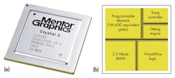
In the first class, the core element is a custom FPGA purposely designed for emulation applications, but a poor choice as a general-purpose FPGA. Mentor Graphics supplies one of these devices, known as the Crystal2, and calls it a “custom emulator-on-chip” (Fig. 1). In the second class, the core element consists of a vast array of simple Boolean processors that execute a design data structure store in a very large memory. Cadence is a supplier and calls it a “processor-based emulator.” Obviously, the custom FPGA-based emulator shares some similarities with the commercial FPGA-based emulator, but still possesses unique capabilities.
The Custom FPGA-Based Emulator
This file type includes high resolution graphics and schematics when applicable.
Originally developed and commercialized by Meta Systems, a French startup acquired by Mentor Graphics in 1996, the custom FPGA-based emulator employed a unique FPGA different from those offered by Xilinx and Altera. It was built on a custom emulator-on-silicon architecture, designed specifically for emulation that encompassed an entire emulator, including configurable elements, a local interconnect matrix, embedded multi-port memories, I/O channels, a debug engine with probing circuitry, and clock generators.
This approach yields three innovations, each offering unique benefits:
• The internal interconnection network of programmable elements
• The external interconnecting network and I/O structure of custom FPGAs
• The DUT debug engine
Internal Interconnection Network Of Programmable Elements
The interconnection network of programmable elements includes two distinct hierarchical layers: a lower layer at the lookup table (LUT) level and at its cluster level, and a higher layer including large blocks of LUT clusters called tiles.
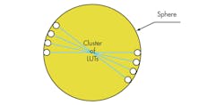
A spatial analogy can describe the lower layer. Assuming that all LUTs are located on the surface of a sphere and the interconnection of any two must cross the center of the sphere, the length of the interconnecting wire is always the same, no matter where two LUTs are located. (Fig. 2).
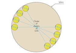
Extending the analogy one hierarchical level higher, clusters of LUTs may be distributed on the surface of a larger sphere and interconnected with the same scheme (Fig. 3). Basically, it’s a fractal graph where the same pattern is repeated, moving from the outside to the inside or from the inside to the outside. The higher layer interconnects tiles with a patented structure that offers similar benefits inherent to the lower layer.
The higher layer interconnects the tiles with a matrix of tiny cross-bars, somewhat analogous to a network-on-chip (NoC) architecture, that sets this structure apart from the traditional mesh interconnection network. This approach ensures predictable, fast, and congestion-free routing.
Furthermore, clock trees are wired on dedicated paths independent from datapaths, leading to predictable and repeatable timing as well as the prevention of timing violations by construction because datapaths are longer than clock paths. Unpredictable timing and hold timing violations mar the viability of commercial FPGAs.
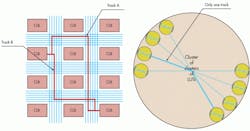
Compared to the structure of a commercial FPGA, the custom approach ensures deterministic and repeatable timing. It removes placement constraints and ensures simple routing and fast compilation (Fig. 4).
The multi-layer interconnection network trades off high capacity, now available in the largest FPGAs, in favor of fast and congestion-free FPGA placing and routing (P&R). It is possible to place and route one custom FPGA in about five minutes. Even by lowering the filling rate of the largest FPGAs to 50% or below, the P&R may take a few hours.
Of course, mapping a billion ASIC-equivalent gate design will require more custom FPGA devices than using the largest commercial FPGAs available today, such as the Xilinx Virtex-7 XC7V2000T. The actual difference may be less than what one could estimate by comparing the internal resources, such as LUTs, since the utilization rate of the custom FPGA is approaching 100% versus 50% or so for the commercial FPGA.
Few factors contribute to mitigate the gap in capacity. They include the built-in VirtualWire logic for I/O maxing instead of consuming LUTs; the built-in debug engine, saving precious configurable resources left to DUT mapping; and an effective router.
Both technologies benefit from distributing P&R on PC farms, but the custom approach still has an edge. Placing and routing a billion ASIC-equivalent gate design on an array of custom FPGAs, performed on a large simulation farm, may take 30 minutes. Placing and routing the same design on a smaller array of Xilinx Virtex-7s will take several hours.
By owning the technology, a supplier of custom FPGA-based emulators controls its destiny and can optimize and customize the P&R software, something the supplier of emulators based on a commercial FPGA cannot. The latter is at the mercy of the FPGA vendor.
External Interconnection Network Of The Emulator-on-Chip
The external interconnection network of the emulator-on-chip is based on a technology called VirtualWire.2 Through VirtualWire, a collection of FPGAs is automatically compiled into a single, giant FPGA untouched by potential timing problems that spoil an array of equivalent FPGAs interconnected via a traditional scheme. At the time the technology was developed, only emulators using commercial FPGAs were available. Today, the same technology is embedded in an emulator-on-chip.
VirtualWire is based on multiple re-synthesis processes (timing, memory, interconnect) that transform a DUT into a functionally equivalent design mapped onto an array of custom emulator-on-chip devices.
Timing re-synthesis uses correctness-preserving transformations to retime a user’s design by introducing a single, high-speed clock to protect it from inaccurate FPGA delays. It also eliminates the hold-time problems of traditional emulation systems.
Memory re-synthesis enables low-cost implementation of memories of all types, including wide multi-ported RAMs, eliminating the need to build custom memory cards or use FPGA memory. Multiplexing and memory sharing allows the use of fast and inexpensive commodity SRAM chips for memory emulation.
Interconnect re-synthesis expands the inter-device communication bandwidth by increasing the number of I/O signals in transit on the fixed and limited number of I/O pins of the device and pipelines connections at maximum speeds. The net result is a swell in the device utilization to about 100%, avoiding congestion and preserving the integrity of the DUT.
The multiplication of I/O signals through each I/O pin appears similar to the method of I/O maxing implemented on FPGA prototyping boards. The VirtualWire implementation is more complex. It offers:
• Global-timing correctness and system scalability by guaranteeing local-timing correctness
• The virtual clock to clock all flip-flops, distributing a single, synchronous, low-skew clock
• Signal routing and scheduling under compiler control because signals must travel through a known number of FPGAs
The VirtualWire implementation also provides bandwidth amplification that leads to higher FPGA and wire utilization. The multiplexing technique amplifies interconnect bandwidth at all packaging levels, from inter-FPGA and inter-board to inter-cabinet, making partitioning easier.
Furthermore, it offers the same multiplexing technique for accessing memory. By multiplexing data buses, wide memories can be built using common SRAM chips. Multi-ported memories can be implemented using SRAM chips. Memory scheduling can be integrated in the routing and scheduling step.
Integrated Design Debugging Capabilities
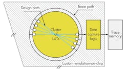
The third innovation involves the integrated design debugging capabilities of the custom approach. Based on on-the-fly smart data capture implemented inside the chip and a trace memory mounted next to each chip on the emulation board, the method guarantees visibility of all elements of the DUT. This is done via construction and not compilation of internal probes. It also avoids degradation in emulation speed.
Total visibility is achieved by connecting all LUTs and embedded memory outputs to on-chip signal probing circuitry in silicon, eluding the need to route them at compilation. In turn, the probing circuitry directs the probe data to a bank of fast memory chips, coupled to the custom emulator-on-chip devices mounted on the emulation board. This reserves routing resources to build the design image, increasing the efficiency of the reconfigurable hardware (Fig. 5).
The design debugging capabilities are augmented by an integrated triggering mechanism and a built-in logic analyzer with a graphical path browser that accelerate the identification of difficult-to-find bugs. The emulator-on-chip enables triggering on registers by default, force-n-release, memory/register peek-and-poke, and save-n-restore.
Drawbacks Of The Emulator-on-chip
Unfortunately, there are drawbacks to the custom approach that stem from the lower capacity density of the custom chip compared to the largest commercial FPGAs. One disadvantage is that to map any given design size, the emulator would need more FPGAs, leading to larger physical dimensions and heavier weight.
Roughly speaking, the dimensions are an order of magnitude larger than those of an emulator based on commercial FPGAs of the same design capacity. The weight is approximately five times heavier. Power consumption is higher, albeit at a lower ratio of about four times more wattage.
The raw clock speed of the commercial FPGA-based emulator is faster. According to public data, it appears to be two times faster than that of the emulator-on-chip. Again, this derives from the difference in capacity of the two chips. In fact, the larger capacity of the off-the-shelf FPGA accommodates bigger portions of the design and allows for fewer devices to fit the entire design. The net result is that interconnecting wires are shorter and propagation delays are faster.
But to take advantage of this capability, time-consuming manual partitioning is always necessary. Without optimizing the partitioning and removing hops—that is, combinational wires crossing multiple FPGAs—the emulation speed may be lower in the commercial FPGA-based emulator. Raw speed is one thing. Actual performance/bandwidth in the real world is another.
References
1. “Four Technologies Converge In Hardware Emulation,” Lauro Rizzatti
2. Virtual Machine Works (VMW) invented VirtualWire in the 1990s. Ikos acquired VMW in 1996. Mentor Graphics acquired Ikos in 2002.
Lauro Rizzatti is a verification consultant. He was formerly general manager of EVE-USA and its vice president of marketing before Synopsys’ acquisition of EVE. Previously, he held positions in management, product marketing, technical marketing, and engineering. He can be reached at [email protected].

