Power Trumps Performance In Today’s SoC Designs

Designing a complex embedded system-on-chip (SoC) today is a multi-pronged challenge. With each successive device generation, more and more capabilities and features must be added. The need to achieve higher performance at lower cost (that is, at lower area) and with lower power consumption has raised the bar for success even higher. In fact, low power consumption today is as important, if not even more important, than high performance.
Types Of Power
A digression is worth taking at this junction. The power dissipated in a design can be divided into two categories: static and dynamic.
This file type includes high resolution graphics and schematics.
Static power is the power consumed by a gate when it is not switching. Currents that flow through the transistors even when they are turned off cause static power. From the system’s functional perspective, static power can be considered wasted energy, as it isn’t used for any useful task. At the 65-nm process node, almost half of a design’s power consumption may be due to static power, and its proportion is increasing as process technology nodes shrink.
Dynamic power is the power dissipated when the circuit is performing some function. It is further divided into two components: switching power and internal power.
Switching power is dissipated when charging and discharging the load capacitance at the cell output. The load capacitance comprises the interconnect (net) capacitance and the gate capacitances to which the net is connected. The amount of switching power depends on the switching activity, which is related to the operating frequency of the cell. The more logic transitions on the cell output, the more switching power increases.
Related Articles
• Companies Ramp Up To Move From 20 nm To The Next Node In 2013
• Manhattan And Mr. Spock Offer Lessons In 3D FinFET Design
• FinFETs Herald A Seismic Shift In Semiconductor Technology
Internal power is consumed within a cell for charging and discharging internal cell capacitances. It also includes short-circuit power. During logic transitions, P-type and N-type transistors are both on simultaneously for a short time, causing direct connection from VDD rail to ground rail.
Unfortunately, the laws of physics now work against the designers’ aims. It was relatively smooth sailing down to the 90-nm node: the lower the geometry, the lower the voltage, the faster the switching, and the lower the power consumption. But as geometries continued shrinking below 90 nm, voltages rapidly approached threshold voltages, and switching times increased. Perversely, lowering threshold voltages substantially increases leakage and switching currents—that is to say, increases in static power and dynamic power consumption, respectively.
Today’s Solutions
To address these challenges, numerous techniques have evolved to reduce power consumption at a given level of performance. Historically, power was saved at the circuit design level, mostly via clock gating techniques and other low-level approaches. Regrettably, by the time the design reaches that low level of description, most power consumption has already been cast in concrete, leaving the designer with rather limited choices to get power under control.
In the embedded design world, where hardware and software coexist, power savings bubbled up the design priority hierarchy and is now considered at all design phases. The real payoff comes much earlier in the game, i.e., during architecture definition. Key architectural decisions can have a dramatic impact, resulting in power savings in the tens of percentage points.
At the system level, design involves hardware as well as software. Now, not only clocks down in the hierarchy are gated, but entire portions of the design higher up the hierarchy are also gated—that is, powered down when they do not contribute to the functionality of the device at any given time. This concept leads to power “islands” that can be turned on or off. Hardware or software (either low-level firmware or application-level software) can control the islands’ power state.
When an island is powered down, all the circuitry goes into an undefined state, raising questions. How does the power island recover from that undefined state when powered up again? How does the neighboring circuitry deal with that state? Does it ignore it, or are there unexpected problems?
This isn’t a concern just for the static situation where one island is on and one is off. Circuitry can change values during the transitions when powering up or down. Any transient state that upsets the neighbors is a problem, and a thorough verification plan must incorporate tests that ensure that everything is well behaved regardless of the power states of the different power islands.
Tools have evolved to manage the power structure, including the creation of two different file formats for expressing power intent: Unified Power Format (UPF) and Common Power Format (CPF). These formats allow designers to define the power islands at a higher level without touching or interfering with the register transfer level (RTL) design description.
The Power-Aware Verification Challenge
Given a design with power islands, it is no longer enough simply to verify that the logic works. A thorough verification plan must include the powering up and down of various blocks. If an application allows this to happen at the software level, then even more verification is needed to test out the various combinations of island power state that might occur.
It’s also not enough to test that things work in the static powered-up and powered-down states. The transition between on and off provides an opportunity for unanticipated electrical harm. It’s relatively easy to figure out what will happen under static conditions. It’s much harder to figure out all the intermediate circuit states that occur while powering up and powering down.
A thorough analysis of the entire power management subsystem necessitates low-level circuit simulation or the use of tools specifically designed for power verification. They provide the sign-off-level assurance that power islands play well together. Unfortunately, such analysis of SoCs including hundreds of millions of gates, and soon billions of gates, requires an immense computational capability for running billions of verification cycles.
Fortuitously, emulation technology comes to the rescue. With the ability to achieve verification speeds that are orders of magnitude faster than possible with software simulation without compromising essential accuracy, the latest generations of emulators can perform power-aware design verification and provide activity reports for power estimation in an acceptable time frame well ahead of tape-out.
Critical goals of such power-aware verification can be accomplished during emulation. Because an emulator only verifies logic, and not actual transistor circuitry, emulation won’t check for analog issues or leakage currents. However, it can model the effects and thereby uncover bugs associated with power gating techniques.
It is possible to verify that the logic of the entire circuit can tolerate different portions of the circuit in undefined states, either as a result of being powered down or as a result of being in transition from power-up to powered-down or vice versa. By intelligently randomizing states in accordance with the power intent expressed in, for example, a Unified Power Format (UPF) file, an emulator with this capability can provide critical assurance that the circuit is robust in the face of these undefined states.
While power-aware emulation doesn’t replace full power analysis, it is yet another easy-to-use tool to help build confidence in an SoC’s ability to perform unperturbed by the powering on and off of different parts of the circuit as designers strive to keep power dissipation as low as possible.
The Power Estimation Challenge
Power-aware design verification helps preserve the integrity of the design functionality when power islands are turned on/off. But it does not address a fundamental problem, namely, estimation of power consumption and its corollary, power optimization.
Based on the definitions in the introduction, we can postulate that the dynamic power consumed by a circuit is proportional to the logic transitions that occur within the circuit when in operation. Therefore, for power estimation and optimization, we need to accurately record the switching activity and feed that activity to the tool performing these power-related tasks.
It is intuitive to assume that the recording accuracy of the switching activity increases as the design description moves from the high level of abstraction down to the gate level or transistor level, since more and more details are available (see the figure).
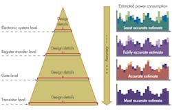
The oxymoron is that at the electronic system level (ESL), when the design is modeled at a high level of abstraction, engineers can enjoy maximum flexibility for comparing multiple architectures, multiple versions, or software algorithms and accomplish the best power optimizations. Unfortunately, the accuracy of power estimation is the lowest. Then at the gate or transistor level, when minuscule details are accessible, very limited flexibility is available to attain anything other than marginal optimizations.
It seems that at the RTL, one can realize the best compromise. Enough details are accessible to achieve suitable estimates of power, and enough flexibility is available to reach sizeable power reduction.
Power consumption is vector dependent, and in the age of embedded SoC designs, it is software dependent. You may need to boot an operating system (OS) and run a set of apps to get a realistic estimate of power consumption.
Verification engines such as simulators and emulators are perfect vehicles to keep track of the switching activity, with the caveat that execution speed degrades—rather dramatically for simulators—moving from a high to low level of design abstraction. The drop in speed becomes painful when there is a need to process several billion cycles to boot an OS and execute a few apps. In fact, only emulators can perform the challenging task in a reasonable time frame.
To alleviate the drop in performance, switching activity is sometimes sampled (once every so many cycles). Regrettably, sampling drops the accuracy of the results and invalidates the task. Sampling is a malpractice that ought to be avoided at all costs.
The switching activity can be tracked on a signal-by-signal basis for the entire run in a switching activity interchange format (SAIF) file or hierarchically on a cycle-by-cycle basis via a fast signal database (FSDB) file. The SAIF file fed into a power estimation tool can help to calculate the average power consumption of the whole circuit except peak power consumption since the cycle-by-cycle information is not tracked. To identify peak power consumption of the entire circuit or of a block, the FSDB file is the proper vehicle since cycle-by-cycle information is now available.
Conclusions
As the mainstream process node moves to 40 nm and as 28-nm, 20-nm, and 14-nm finFETs gain momentum, the largest designs are approaching billion-gate capacities. The time spent in embedded software development is well ahead of the time spent in designing hardware.
According to recent surveys of the semiconductor engineering community, about a quarter of design time is spent meeting power specifications, and close to half of the respondents claimed to implement RTL power optimizations. The surveys also pointed out that the two most popular methods to reduce power are clock gating, in the first position leading the pack by a wide margin, and power gating, in second position and rapidly distancing all other practices.
These trends make power-aware verification and switching activity tracking for power estimation extremely compute-intensive tasks that can only be addressed by the latest generations of emulators.
Lauro Rizzatti is the senior director of marketing for emulation at Synopsys. He joined Synopsys via the acquisition of EVE. Prior to the acquisition, he was general manager of EVE-USA and marketing VP. In the past, he held positions in management, product marketing, technical marketing, and engineering. He can be reached at [email protected].
This file type includes high resolution graphics and schematics.
About the Author

Lauro Rizzatti
Business Advisor to VSORA
Lauro Rizzatti is a business advisor to VSORA, an innovative startup offering silicon IP solutions and silicon chips, and a noted verification consultant and industry expert on hardware emulation. Previously, he held positions in management, product marketing, technical marketing and engineering.
Comment About the Article
To join the conversation, and become an exclusive member of Electronic Design, create an account today!

Leaders relevant to this article: