RISC-V is on the rise, as highlighted by the RISC-V Workshop. Multicore, 64-bit versions of RISC-V are available, and there’s support for FPGA and eFPGA versions.
I’ve been following the RISC-V movement almost since its inception, and had a chance to try out SiFive’s Arduino-compatible HiFive1 board earlier. It contains a 32-bit, SiFive E310 RISC-V-compatible processor. I say compatible because RISC-V defines an instruction set architecture (ISA), not a processor architecture like one of the Arm Cortex-M architectures. Those define how the architecture is implemented and run an Arm-compatible ISA.
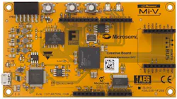
This time around, I took advantage of Microsemi’s Mi-V ecosystem and Future Electronics’ $99 Microsemi Creative Board (Fig. 1). This is a general FPGA development platform, but is one that the Mi-V ecosystem targets for RISC-V deployment. The board I used had an M2GL025 IGLOO2 FPGA. I also had a 2.8-in Touch LCD Display Shield for Arduino that costs about $20. It has a 320- × 240-pixel resolution with a resistive touchscreen and an SPI interface. It’s used by the tic-tac-toe demo.
1. The Microsemi Creative Board from Future Electronics contains an IGLOO2 or SmartFusion2 FPGA. It has connectors for a Pmod, mikroBUS, and Arduino Shield.
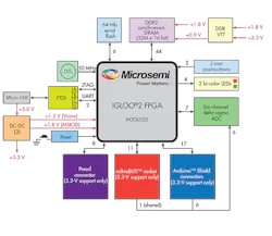
The Creative Board has connectors for a Pmod, mikroBUS, and Arduino Shield (Fig. 2). It also adds a six-channel, sigma-delta analog-to-digital converter (ADC), a 64-Mb serial flash, and 64 MB of DDR2 memory. The serial flash is for application storage, as the FPGAs are flash-based with their own on-board flash memory. RAM-based FPGAs require off-chip flash storage and often use serial flash devices. Flash-based FPGAs start up almost instantaneously, while RAM-based FPGAs need to load the configuration memory from serial flash first.
2. The Creative Board also adds a six-channel, sigma-delta ADC, a 64-M serial flash and 64 MB of DDR2 memory.
The Mi-V ecosystem can be approached in one of two ways. The first is to use predefined FPGA configurations so that developers can start programming a RISC-V system almost immediately. Essentially a developer will only need to be familiar with an IDE. The second is where a more customized version of the system is built, which requires modifying the system design. I took a look at both.
Getting Started
The board doesn’t come with software—it must be downloaded from the Microsemi Mi-V website. The two main components required for software developers are the Eclipse-based SoftConsole IDE and the FPGA flash programmer. The flash programmer is used to download systems into the FPGA. A number of predefined systems on the site include different RISC-V cores and peripheral sets designed to work with the match software applications.
The documentation addresses the operation of the flash programming software and describes the functionality of some of the prepackaged software combinations. This is essentially the Hello World for FPGAs.
I could turn my attention to C code and the SoftConsole IDE once the FPGA on the board was programmed with one of the canned designs. These designs typically include a RISC-V core plus a few peripherals like LED drivers and a UART. They are more than sufficient for writing RISC-V-based applications to test out the system, and often define sufficient peripherals for building an application.
We start by opening one of the test projects in the IDE and connecting the debugger to the board. It was then a matter of compiling and downloading the RISC-V code and firing up the debugger. At this point, the exercise was similar to using the HiFive1 board.
You can build off the sample applications or start from scratch. The predefined RISC-V configurations will handle the operating systems that support RISC-V, including Amazon’s AWS FreeRTOS, Huawei LiteOS, Silicon Labs’ Micrium µC/OS III, and Express Logic’s ThreadX.
As with most embedded systems, developers will need to keep an eye on resource utilization. In this case, it will be program storage and RAM. FPGA utilization will also be part of the mix if additional peripherals are added.
Changing the System
This is where things get interesting and also more complex. Working with FPGAs has become significantly easier, but good FPGA design still requires experience. This is especially true if custom logic will be added, because the designer needs to know how to define and debug it, as well as understand how it will interface to the rest of the system, including the RISC-V core.
There’s a very nice caveat, though. Adding predefined peripherals like a UART or two only requires connecting these new devices to the appropriate control logic that already exists in most of these designs that utilize the AMBA AXI bus protocols. That’s because the predefined systems already include this support and it is relatively easy to add when starting with a new project.
A good place to start for neophytes is the Polarfire FPGA Building a RISC-V Processor Subsystem tutorial. This actually describes the process targeting a new Microsemi Polarfire FPGA, but the process is almost identical for the IGLOO2. Only the initial component selection changes, along with a flag that needs to be added in one of the constraint files.
My IGLOO2 kit has its own section on github. This is where the example projects are found, as well as instructions for modifying the FPGA configuration. You will also need the RISC-V Junk Drawer project. In addition, read the note at the very bottom of the Modify_The_FPGA_Design subproject. You need to uncomment the `define USE_REGISTERS statement in the file coreriscv_axi4_defines.v because the default configuration targets a larger FPGA than the IGLOO2 that’s on the board.
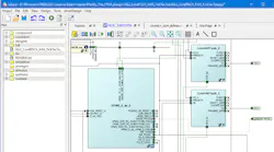
3. The Libero SoC FPGA IDE was used to add two more UARTs to the mix.
I added two additional UARTs to the mix (Fig. 3). That was relatively easy since one was already in the sample design. I didn’t get to test them with another device, since the I/O pins weren’t accessible, but I was able to configure them in software. You may develop something more useful.
Adding the UARTs is relatively easy. It requires definition of the I/O pins to use and subsequently linking the UART I/O to the AMBA AXI bus so that it can be accessed, and then to the pins. There’s some system and clock I/O, too.
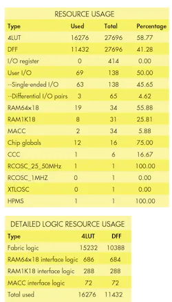
After that, it was simply a matter of rebuilding the project and downloading it to the FPGA. Even adding a couple of UARTs didn’t make a significant dent into the FPGA’s gate count (Fig. 4). More than half the LUTs and RAM were used, but a lot of logic and storage is left over.
4. This is from the resource usage report after adding a second and third UART to the tic-tac-toe design.
Overall, the installation and testing of examples plus adding the UARTs, took a couple of days. The actual download and working with the IDE required a fraction of that time. Anyone familiar with Libero had done it much more quickly. Those new to FPGAs will want to take more time.
Likewise, those wanting to incorporate custom logic could use some training or be prepared for a good bit of reading and experimentation. It’s a bit more complicated than rewiring a plug board. Issues such as timing, loading, and layout issues tend to be fewer when dealing with a smaller FPGA like the IGLOO2, so it’s a good one to learn. Of course, more ambitious projects can be tackled using a Polarfire FPGA.
It will be interesting to see what other projects are posted in the future. The platform provides sufficient room for growth, and to do some interesting projects that take advantage of an FPGA. The multiple expansion sockets also make it easy to add sensors and controls to the system.
Let me know how you fare with the Microsemi Creative Board.
About the Author
William G. Wong
Senior Content Director - Electronic Design and Microwaves & RF
I am Editor of Electronic Design focusing on embedded, software, and systems. As Senior Content Director, I also manage Microwaves & RF and I work with a great team of editors to provide engineers, programmers, developers and technical managers with interesting and useful articles and videos on a regular basis. Check out our free newsletters to see the latest content.
You can send press releases for new products for possible coverage on the website. I am also interested in receiving contributed articles for publishing on our website. Use our template and send to me along with a signed release form.
Check out my blog, AltEmbedded on Electronic Design, as well as his latest articles on this site that are listed below.
You can visit my social media via these links:
- AltEmbedded on Electronic Design
- Bill Wong on Facebook
- @AltEmbedded on Twitter
- Bill Wong on LinkedIn
I earned a Bachelor of Electrical Engineering at the Georgia Institute of Technology and a Masters in Computer Science from Rutgers University. I still do a bit of programming using everything from C and C++ to Rust and Ada/SPARK. I do a bit of PHP programming for Drupal websites. I have posted a few Drupal modules.
I still get a hand on software and electronic hardware. Some of this can be found on our Kit Close-Up video series. You can also see me on many of our TechXchange Talk videos. I am interested in a range of projects from robotics to artificial intelligence.
Voice Your Opinion!
To join the conversation, and become an exclusive member of Electronic Design, create an account today!

Leaders relevant to this article:


