This file type includes high resolution graphics and schematics when applicable.
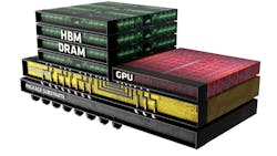
One can never have enough storage and chip designers have been working hard to deliver as much storage as possible. Almost every avenue is being pursued, from Nantero's nanotube-based NRAM (see “Non-Volatile NRAM Nanotubes Deliver Endurance and Performance” ) to AMD’s 3D High Bandwidth Memory (HBM) chip architecture (Fig. 1). New technologies like NRAM, MRAM, and FRAM deliver non-volatility to challenge not only flash memory, but DRAM.
The move from conventional single-die chip storage to 3D multi-die continues (Fig. 2). It pays to limit interconnect runs as speeds and capacity increase rapidly. Moving storage closer to the processor is important to performance and it is occurring at all levels such as Diablo Technologies’ Memory Channel Storage that moves flash memory onto the DRAM memory channel (see “Memory Channel Flash Storage Provides Fast RAM Mirroring” ).

3D Architectures
Using multiple dies in the same package allows a designer to mix different chip technologies easily. It is also a way to increase the packing density to improve capacity. It can also provide a performance by reducing interconnect length and allowing higher-speed transfers, since designers have better control over the connections.
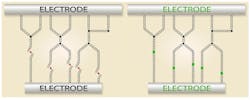
Multiple dies on a chip have been commonly available for many years, but they were often used in areas where their higher cost could be justified by the added performance and reliability. A chip carrier would typically be wired internally in a fashion similar to connecting a die to external pins.
Die stacking has also become common because of the tight spaces required by smartphones and other mobile devices. Microcontrollers incorporate flash memory and RAM on chip, but these are often separate chips for more powerful microprocessors. Stacking a flash memory and DRAM die on top of a microprocessor die cuts down on space while providing a more reliable platform. Again, the wiring between chips is similar or identical to the chip-to-carrier connection.
The use of silicon interposer layers with through-silicon vias (TSVs) lets designers drop down multiple chips, but the approach is more akin to a silicon circuit board than the multichip carriers. The latter requires wiring to connect the chips together and to the outside world.
The use of interposers has been pushed by FPGA vendors such as Xilinx and Altera. Xilinx originally called the technology 2.5D (see “10,000 Connections Between FPGA Slices” ), but these days everyone refers to it as 3D. Xilinx initially used this approach to provide more logic elements using multiple FPGA die. They also paired it with high-speed SERDES die that used different silicon technology.

Altera’s Stratix 10 uses a similar approach, but delivers 5.5 million logic elements and a quad-core Cortex-A53 complex on a single die. Altera’s SERDES die are connected using a layer that Altera calls the Embedded Multi-die Interconnect Bridge (EMIB). The main difference is that the EMIB is a small set of connections that link the FPGA die to adjacent dies called Tiles (Fig. 3). EMIB provides higher performance because of its 2-layer design and shorter connections. It also costs less than a full silicon interposer approach. Altera plans on having different I/O Tiles for application-specific interfaces.
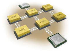
A number of vendors are doing 3D on the vertical side. The Hybrid memory cube (HMC) addresses the RAM side of storage (see “Hybrid Memory Cube Shows New Direction for High-Performance Storage” ). It stacks die using TSV connections. The base layer is the controller that has multiple, high-speed SERDES linking it to one or more hosts. The HMC specification addresses a range of configurations from a simple single-port connection to one host to multiport connections (Fig. 4). It targets enterprise servers where the demand for RAM is insatiable.
The appetite for flash storage is equally insatiable. Single-level cell (SLC) has given way to 2-bit multi-level cell (MLC) and 3-bit triple-level cell (TLC). The tradeoffs between SLC, MLC, and TLC tend to be space and capacity versus write speed and write lifetime.
Samsung V-NAND, also known as vertical NAND, is a 32-layer TLC device (Fig. 5). It provides the highest storage density at this point (see “Mass Production Underway for 32-Layer 3D V-NAND Flash” ). Identical dies are stacked on top of each other. Samsung’s SSD 850 EVO line is the initial home for V-NAND. This includes an M.2 and mSATA versions. That later has a capacity up to 1 Tbyte using a 6 Gbit/s SATA interface.
AMD’s high bandwidth memory (HBM) combines the interposer and vertical stacking. CPU and GPU dies are single-layer, but the memory is a stack of multiple RAM die. HBM has a significant advantage over HMC. It does not have to transfer data using high-speed SERDES. Instead, data can be moved in parallel.
HBM will first find a home in AMD’s Radeon R9 Fury X GPU card. This will have 4 Gbytes of HBM plus the latest Fiji GPU from AMD with 4,096 stream processors, 64 GCN (graphics core next), 128 render output units, and 256 texture mapping units.
The memory interface is 4,096 bits wide. The GPU delivers 8.6 FLOPS while only having a TDP of 300 W. This is only 10 W more than the earlier Radeon R9 290X while improving performance by more than 50%.
Nonvolatile Memory Technologies
Packaging technologies are one way to improve storage density and performance. Changing the storage technology is another that is complementary to the packaging. There are quite a few technologies that have been around and found a niche as well as emerging technologies. All look to take away all or part of the market from SRAM/DRAM and flash memory. These technologies include various resistive RAM approaches, FRAM, and MRAM.
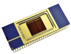
Nantero’s NRAM is a new resistive memory technology that uses nanotubes (Fig. 6). It meshes well with current CMOS fab technology and it has impressive retention and performance specifications. It should retain data at room temperature for over 1,000 years. It can handle extended temperature ranges with lower retention capability. It should scale to 5 nm and it can handle 3D structures and MLC support. It is based on a crossed nanotube (CNT) film deposited on a silicon substrate.
Crossbar’s resistive RAM is similar (see “RRAM Challenges Flash Storage” on electronicdesign.com). It uses a switching medium that includes metal filaments with metal ions migrated from one end to another to change state. It has a 10-year retention and support for MLC and TLC techniques as well as 3D stacking. It is 20 times faster than flash and has endurance support of over 10,000 cycles.
FRAM has been showing up in quite a few of Texas Instruments’ (TI) MSP430 microcontrollers (see “Low-Power Microcontroller Has Up to 128 Kbytes of FRAM” ). It has replaced SRAM and flash storage on some models. TI also has a set of routines the can save and restore system settings to FRAM that are not stored in FRAM. This can include system settings like status and control registers for peripherals.
The Compute Through Power Loss (CTPL) utility API allows an almost instant-on capability since the application stack and status are kept in the nonvolatile FRAM. A sleeping system automatically restores these settings on power-up.
Everspin MRAM is similar to FRAM functionality, but uses a much different storage mechanism for its magnetic tunnel junction (see “Q&A: Everspin Takes MRAM to the Mainstream” ). It has a data retention of more than 20 years with a 35 ns read/write time. It has unlimited endurance, making it a good choice for a number of applications like RAID controller cache. The latest products employ Spin-Torque MRAM (ST-MRAM), which allow it to be used in DDR3 systems. Everspin also has parallel and SPI MRAM products. The current chip capacity is 64 Mbits.
Phase change memory (PCM) originally utilized behavior of chalcogenide glass. Micron has phased out its commercial PCM line based on technology acquired from Numonyx. Research is ongoing, so the technology may resurface in the commercial space in the future.
New Flash Configurations
DRAM and flash memory in general remain the dominant force in storage. Flash memory has pushed rotating magnetic media into more niche markets as end-user devices have moved to mobile platforms requiring more compact and power-sipping flash storage. Large hard disks are still part of enterprise solutions, set-top box recorders, and PC backup, but flash memory has moved from its niche into the primary nonvolatile storage mechanism in most areas. Flash memory’s ability to fit into almost any space makes it a much better choice than a hard disk for a growing number of applications, including wearable tech (see “Wearing Your Technology” ).
Diablo Technologies’ Memory Channel Storage (MCS) moves flash memory to the memory channel of high-performance microprocessors. It licenses its technology to companies ranging from SanDisk to IBM that deliver DDR3 and DDR4 modules that compete with DRAM for slots on the motherboard. The DIMM modules use the same interface, but the transactions are more like flash-memory storage devices rather than DRAM since the write speeds for flash are significantly slower.
MCS storage can be utilized as a block device, essentially providing a faster transfer rate to the system since the memory channel has a higher bandwidth than other I/O interfaces and there is less system overhead. MCS storage has a smaller transaction size than block devices that are designed to accommodate blocks of data on rotating magnetic media. The C2 version of MCS has a feature called NanoCommit that moves the minimum transfer size to a CPU cache line. This allows mirroring of key data structures, allowing significant performance improvements for applications like database servers.
This file type includes high resolution graphics and schematics when applicable.
DRAM still tends to be faster and larger than other technologies to date. It is one reason that nonvolatile DRAM has emerged in enterprise environments where reliability is critical. Viking Technology’s ArxCis-NV is a hybrid DIMM with DRAM and flash memory on-board (see “Non-Volatile DIMMs and NVMe Spice Up the Flash-Memory Summit” ). The flash memory is used to retain the DRAM contents when the system is powered down. A supercap provides power in the event of system power, loss allowing the on-board controller to copy DRAM to flash memory. DDR3 and DDR4 versions are available.
There is never a dull moment when it comes to storage technology. The mix of new storage technologies and packaging techniques provides designers with a wide range of options.
About the Author

William G. Wong
Senior Content Director - Electronic Design and Microwaves & RF
I am Editor of Electronic Design focusing on embedded, software, and systems. As Senior Content Director, I also manage Microwaves & RF and I work with a great team of editors to provide engineers, programmers, developers and technical managers with interesting and useful articles and videos on a regular basis. Check out our free newsletters to see the latest content.
You can send press releases for new products for possible coverage on the website. I am also interested in receiving contributed articles for publishing on our website. Use our template and send to me along with a signed release form.
Check out my blog, AltEmbedded on Electronic Design, as well as his latest articles on this site that are listed below.
You can visit my social media via these links:
- AltEmbedded on Electronic Design
- Bill Wong on Facebook
- @AltEmbedded on Twitter
- Bill Wong on LinkedIn
I earned a Bachelor of Electrical Engineering at the Georgia Institute of Technology and a Masters in Computer Science from Rutgers University. I still do a bit of programming using everything from C and C++ to Rust and Ada/SPARK. I do a bit of PHP programming for Drupal websites. I have posted a few Drupal modules.
I still get a hand on software and electronic hardware. Some of this can be found on our Kit Close-Up video series. You can also see me on many of our TechXchange Talk videos. I am interested in a range of projects from robotics to artificial intelligence.
Comment About the Article
To join the conversation, and become an exclusive member of Electronic Design, create an account today!

Leaders relevant to this article: