IBIS Modeling (Part 3): How to Achieve a Quality Level 3 IBIS Model via Bench Measurement
This article is part of the Test & Measurement library series: Simulate Your Way to Design Success with IBIS Modeling.
Members can download this article in PDF format.
What you'll learn:
- The different IBIS quality levels.
- The steps in the IBIS bench measurement procedure.
- Process for Quality Level 2a and Level 2b validation.
The Input/Output Buffer Information Specification (IBIS) is a behavioral model that’s gaining worldwide popularity as a standard format to generate device models. The device model’s accuracy depends on the quality of the IBIS models offered by the industry. Therefore, providing quality, reliable IBIS models for signal-integrity simulations is a strong commitment to the customer.
One way to generate IBIS models is through simulations. However, in some cases, the design files aren’t available, making it impossible to generate IBIS models from simulation results. In such instances, generating IBIS models via bench measurement can fill that gap, offering a high-quality and more realistic device behavioral model.
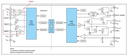
Figure 1 shows the complete stage in generating IBIS models through bench measurement. Using the actual silicon, the device’s receiver and driver buffer behaviors are extracted to represent the current vs. voltage (I-V) data and the voltage vs. time (V-t) data.
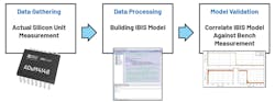
The model will then be validated against an actual bench setup with complete loading conditions. This procedure provides a Quality Level 2b IBIS model. To achieve the higher Quality Level 3 model, the generated IBIS model also will be validated against the device’s transistor-level design with the recommended loading conditions.
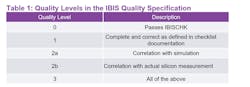
To characterize the quality, the IBIS Quality Task Group has formulated a quality-control (QC) process using five QC stages. They developed a checklist to define different quality levels (Table 1).
The quality levels presented in Table 1 provide a standard for IBIS model quality, which varies from vendor to vendor.1 Having a standard for IBIS model accuracy will ensure customers that they’re getting accurate and reliable models. The higher the quality level of the model, the more accurate its data since higher quality levels require more validation processes.
Based on the book Semiconductor Modeling: For Simulating Signal, Power, and Electromagnetic Integrity by Roy Leventhal and Lynne Green,2 there are five recognized quality levels of the IBIS correctness checklist:
Quality Level 0—Passes IBISCHK
A Quality Level 0 requirement should at least pass the IBIS parser. IBISCHK must yield zero errors, and all warnings must be explained if they can’t be eliminated. Ideally, there should be no warnings, but it’s recognized that some warnings can’t be removed. The “Error,” “Warning,” and “Note” messages from the parser check serve as guides for the IBIS model maker to identify errors and easily correct them. Figure 2 shows the IBIS model parser check.
Quality Level 1—Complete and Correct as Defined in Checklist Documentation
A Quality Level 1 IBIS model passes Quality Level 0 with an additional check for correctness and completeness of a basic simulation test. It includes the correctly defined package parasitic, pin configuration, and load parameters. Ramp rate and typical/minimum/maximum values must be in accordance with the device specifications. The detailed requirements under Quality Level 1 found here also can be used as a reference.
Quality Level 2a—Correlation with Simulation
Quality Level 2a compares the performance of an IBIS model to the device’s transistor-level design. The IBIS model’s performance when connected to a load is correlated against the device’s transistor-level design with the same load. The results from the two simulation setups are then compared and checked if the model passes Quality Level 2a. Details are discussed in the section “Validation and Results.”
Quality Level 2b—Correlation with Actual Silicon Measurement
Quality Level 2b compares the performance of an IBIS model against the device’s actual unit. Like Quality Level 2a, the same load must be connected to the two setups during correlation. The model will pass as a Quality Level 2b based on the correlation results. Details will be discussed in the section “Validation and Results.”
Quality Level 3—Correlation of Transistor-Level Simulation and IBIS Bench Measurement
Quality Level 3 specifies that the IBIS model is validated against the transistor-level design and the actual unit. For the model to pass Quality Level 3, it must pass the correlation for both Quality Levels 2a and 2b. On top of that, the model must pass the IBIS parser test (Quality Level 0) and satisfy the IBIS quality checklist (Quality Level 1). Details will be discussed in the section “Validation and Results.”
The Use Case
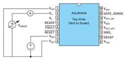
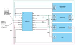
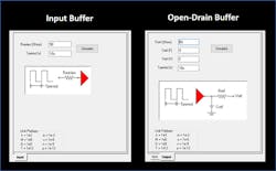
In this article, the case under study is the ADuM4146, an isolated gate driver specifically optimized for driving silicon-carbide (SiC) MOSFETs. The ADuM4146 has three input pins (VIP, VIN, and /RESET) and two open-drain pins (READY and /FAULT), but this article only discusses one pin for each buffer type (Fig. 3). It’s because the procedure for building and validating the IBIS models for pins with similar buffer types is the same. The VIP pin will be used as the use case for the input buffer, and /FAULT will be employed as the use case for the open-drain buffer.
It's important to note that although similar buffer types have the same IBIS modeling procedure and validation, it doesn’t necessarily mean that they have the same IBIS data. The article only discusses one pin per buffer type to simplify the explanation of building the IBIS model and validation process.
The ADuM4146 has a standard small outline wide-body package (SOIC_W), which is represented as a resistor, inductor, and capacitor (RLC) parasitic in the validation process. The package RLC values were extracted through simulations by a package engineer. The dedicated printed circuit board (PCB) has a similar case to the package parasitic: It’s represented by the RLC parasitic, and the values were extracted by a PCB engineer.
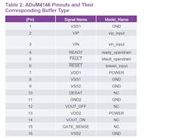
Table 2 shows the ADuM4146 pin configuration and the corresponding buffer type for each pin. This information will be used in the [Pin] keyword of the IBIS model.
IBIS Bench Measurement Procedure
Gathering data through bench measurement may be affected by different external factors. These factors should be compensated to achieve correlation and provide quality models.
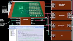
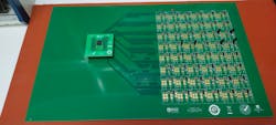
To minimize the effect of external factors, the device under test (DUT) is placed on a dedicated fixture, which aims to reduce unwanted capacitance that may cause inaccuracy to the measured device behaviors (Fig. 4). Parasitic capacitance is a significant problem in actual silicon measurement and is often the factor limiting the operating frequency and bandwidth of a device model.
What follows are the steps for generating an IBIS model through bench measurement:
1. Prepare the Setup
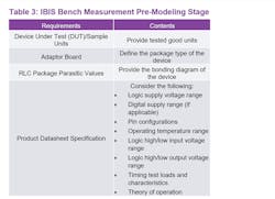
Table 3 shows the IBIS pre-modeling stage requirements for bench measurement, and Table 4 shows the different model types and model components that define the buffer behavior. The model types are discussed in detail in Parts 1 and 2 of this article series. You also can refer to the IBIS Modeling Cookbook.3
2. Bench Setup
Understanding how the device operates is essential in data gathering for IBIS models. As shown in Figure 1, this is the first stage. It’s accomplished by extracting the I-V data and the V-t data. Both are represented in tabular form.
I-V data includes the ESD clamp behavior and the driver strength, while the V-t data indicates the transition from low state to high state and vice versa. The switching behavior is measured with a load connected to the output pin, equivalent to the value that the output buffer will drive. Nevertheless, the usual load value is 50 Ω to represent the typical transmission-line impedance.
For I-V measurement, a programmable power supply capable of sinking and sourcing current and a curve tracer are used to sweep the voltage and gather the current behavior of the buffer. The data is recommended to be taken in the voltage range of –VDD to 2 × VDD, and the typical, minimum, and maximum corners. V-t measurement requires the use of the oscilloscope with appropriate bandwidth and a low-capacitance probe.
The DUT, mounted on the dedicated fixture, is to be tested under varying temperature conditions with the use of a temperature forcing system to capture the minimum, typical, and maximum performance. In this case, the minimum (weakest drive strength, slowest edge) data is taken at 125°C, and the maximum (strongest drive strength, fastest edge) data is taken at –40°C.
3. Bench Data Extraction
Once verified that the bench setup is ready, the process of gathering the required I-V and V-t data can begin. Output and I/O buffers demand both I-V tables and rise/fall data, while input buffers only demand I-V tables.
I-V (Current vs. Voltage) Data Measurement
The I-V curve measurements cover the four IBIS keywords—[Pullup] and [Pulldown] represent the I-V behavior of the pull-up component when driving high and the pull-down component when driving low, while [Power Clamp] and [GND Clamp] represent the I-V behavior of the ESD protection diodes during the high-impedance state.
To measure the I-V characteristics, mount the component on the dedicated board and connect the power and ground pins to the power supply. Prepare the temperature forcing system, adjust to the desired temperature, and wait for it to stabilize. Sweep the voltage within the recommended range, then, using the curve tracer, measure the current of the required buffer.
The positive node of the sweeping device for pull-up and power-clamp data should be connected to the supply voltage and the negative node should be connected to the pin, while the sweeping device for pull-down and ground-clamp data are referenced to ground. Extrapolation may be required at times when the curve tracer isn’t able to sweep the entire range.
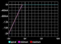
Figure 5 shows the bench setup for input buffer (VI+) I-V ground-clamp measurement, while Figure 6 shows its measured behavior. The ground-clamp circuit is triggered when the input goes below ground resulting in a negative current, and then approaches and settles at zero. The input pin (VIP) doesn’t have a power-clamp component, so its model will not have power-clamp data.
The same method is implemented to the ESD clamp, pull-up, and pull-down data of the output buffer. In this case, though, the ADuM4146 READY and FAULT pins are open-drain buffers. Thus, they don’t have a pull-up component and only require pull-down data.
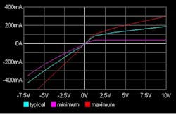
Figure 7 shows the ADuM4146 open-drain buffer’s pull-down data result. The pull-down curve starts from a negative current, then crosses zero going to the positive quadrant, also in the range of –VDD to 2 × VDD.
Buffer Capacitance (C_comp) Extraction
According to the IBIS Modeling Cookbook for IBIS Version 4.0, “The total die capacitance of each pad, or the C_comp parameter, is the capacitance seen when looking from the pad into the buffer for a fully placed and routed buffer design, exclusive of package effects.”5 One way to obtain the C_comp value is by using following equation:
C_comp = CIN − Cpkg
where CIN = device input capacitance, and Cpkg = device package capacitance.
V-t (Output Voltage vs. Time) Data Measurement
The V-t curve measurements also cover four IBIS keywords: [Rising Vddref] and [Falling Vddref] pertain to the transitions from low-to-high and high-to-low with load referenced to the supply, while [Rising Gndref] and [Falling Gndref] pertain to the transitions from low-to-high and high-to-low with load referenced to the ground. Related to these is the keyword [Ramp], which defines the transition rate when changing from one state to another, taken at 20% to 80% of the waveform.
Measuring the rise and fall time data requires the use of an oscilloscope on the buffer driving the required load. In this case, a 50-Ω resistor is utilized to represent the transmission-line impedance. For the open-drain type, connect the load to the buffer and the supply voltage to measure the switching behavior with reference to VDD1. Be sure to stabilize the temperature as required using the temperature forcing system to capture the minimum, typical, and maximum range.
Figure 8 shows the ADuM4146 actual bench setup for the READY and /FAULT pin’s switching behaviors. Given that ADuM4146 digital output pins are open drain, only the rising and falling behaviors referenced to the supply voltage are required.
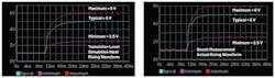
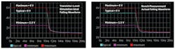
Figures 9 and 10 show the captured rising and falling waveforms for the /FAULT pin both in transistor-level simulation and actual simulation measurement. Both setups use the same loading conditions of 50 Ω connected to VDD1, across typical, minimum, and maximum corners.
4. Building the IBIS Model
The next stage in creating an IBIS model is processing the gathered data and building the model itself. In this stage, the raw data tables are inserted in an IBIS text format following the necessary keywords and including the device parameters. The detailed process for this is discussed in Part 1 of this article series.
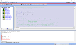
Figure 11 shows the ADuM4146 IBIS model generated from bench measurement. The model should pass the IBIS parser, which includes basic checks such as matching between the I-V and V-t tables and reviewing the monotonicity of table data. All errors, warnings, and notes should be completely resolved before continuing with the validation process. In addition, the model should satisfy the IBIS quality checklist.
Validation and Results
The validation process of this article will follow the one presented in Part 2 of this series. More details regarding the validation process of an IBIS model are discussed there.
The model must first pass the parser test, which can be checked using software with integrated IBISCHK or applying the open-source executable code from ibis.org. After passing the parser test, the model must then be correlated against either its transistor-level schematic or the actual silicon unit.
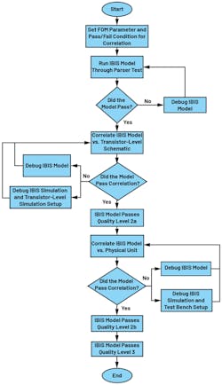
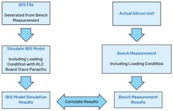
Since this article aims to achieve the Quality Level 3 model, ADuM4146’s IBIS model will be correlated against both its transistor-level schematic and actual unit. The figure of merit (FOM) value will be set to determine whether the IBIS model will pass both correlations. In this case, the FOM value for both correlations must be greater than or equal to 95% to pass the Quality Level 3 IBIS model validation. Figure 12 presents a flowchart diagram of the validation process that an IBIS model must go through to pass Quality Level 3.
The area under the curve metric will be used to compute the FOM values of both correlations. The same loading conditions must be placed on the two sets of correlation. During validation, it’s advisable to follow the loading conditions indicated in the datasheet to test the device in its normal operation.
To correctly validate the IBIS model against a reference—for example, IBIS vs. bench measurement correlation—the PCB traces that the signal will go through in the bench measurement setup must be added to the IBIS simulation setup.
Below are the two conditions performed to achieve the Quality Level 3 IBIS model.
IBIS Quality Level 2a Validation
Figure 13 shows the IBIS model Quality Level 2a validation process. This correlation process intends to assess the degree to which the IBIS model data will result in simulations that match the transistor-level simulation results.
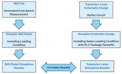
Figure 14 shows the ADuM4146’s IBIS model simulation setup for both its input and open-drain buffers with loading conditions.
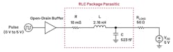
Figures 15 and 16 show the transistor-level design simulation setup with loading conditions for input and open-drain buffers, respectively. The package RLC values of the device are added in between the buffer and the load to replicate the package parasitic in the IBIS setup.
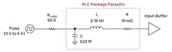
Figures 17 and 18 show the correlation results of both input and open-drain buffers, respectively, when running the IBIS model with a standard load and comparing the results against a transistor-level reference simulation using the same load. A 50-Ω resistor is used as a load for the IBIS vs. transistor-level correlation setups of the open-drain buffer. A transient analysis is performed for both setups with a 10-μs pulse input.
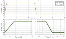
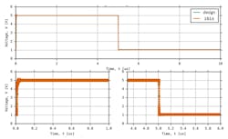
Table 5 shows the computed FOM values for the two buffer models when correlated against their transistor-level schematic. Since both buffer models have FOM values greater than 95%, the IBIS model passes Quality Level 2a.

IBIS Quality Level 2b Validation
IBIS Quality Level 2b requires the model to be correlated against bench measurement. Therefore, factors that may affect the performance of bench measurement should be considered.
The main challenge when performing bench measurement is signal attenuation, which is mostly caused by trace parasitics. When measuring data from the actual unit, it’s best to use a dedicated board with a low-capacitance probe to reduce the effects of trace parasitics as much as possible.
In this case, the IBIS bench dedicated board was a solution for signal-integrity issues, reducing attenuation caused by unwanted signals that might get introduced to the signal of interest. Figure 19 shows the validation process for IBIS Quality Level 2b.
The main objective in the IBIS model correlation is to obtain results that are as close as possible to the reference. In capturing rise/fall-time data in the oscilloscope, it’s best to use a probe with extremely low loading to reduce signal attenuation. The errors introduced by the probe and instrument combination can significantly contribute to the signal of interest.
According to Tektronix, “Special filtering techniques and proper selection of tools to de-embed the measurement system’s effects on the signal, displaying edge times, and other signal characteristics are key factors to consider when measuring the actual silicon performance.”4
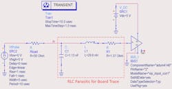
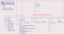
Figures 20 and 21 show the simulation setups of the IBIS models with input and open-drain buffers, respectively, considering the loading conditions. The RLC values connected in series to the buffers are the parasitic values from the board traces. It’s important to consider their effect on the model’s performance when adding any loading by the fixture to replicate the lab setup.
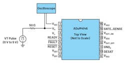
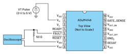
Figures 22 and 23 present a diagram representation of the bench setups with loading conditions for input and open-drain buffers, respectively. A 5-V pulse signal is used to drive the open-drain buffer, which is connected to a 50-Ω load.
Correlation results for IBIS simulation and bench measurement of input and open-drain buffers are shown in Figures 24 and 25, respectively.
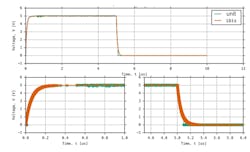
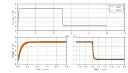
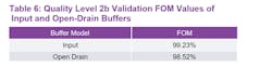
Table 6 shows the FOM values of input and open-drain buffers when correlated against the actual silicon bench measurements. The FOM values are greater than 95%, which means that the IBIS models of the two buffers pass Quality Level 2b. Since the model passes Quality Level 2a and Quality Level 2b, it can now be considered as a Quality Level 3 IBIS model.
Conclusion and Takeaway
Extracting the data necessary for hardware-to-model correlation is one of the most challenging procedures in building a quality IBIS model through bench measurement. By careful attention to detail and understanding the behavior of the I/O circuit, it’s possible to achieve a close correlation between the lab measurements and IBIS simulation results.
Eliminating as much attenuation as possible is key to having a high FOM value in correlation. Considering this, it’s advisable to use a dedicated test fixture with well-matched equipment and accessories to ensure the integrity of the signal.
It’s also important to keep in mind that in correlation, the IBIS model and reference setups must be identical in terms of the traces that the signal will go through. This decreases the error caused in the correlation; thus, increasing the FOM value.
Having an IBIS Quality Level 3 model is an advantage for both semiconductor vendors and customers. This ensures having a higher accuracy level of the model when it was validated from pre-silicon to actual silicon measurements.
Acknowledgements
We would like to thank the ADI design engineers, ADGT test development engineer, and ISO team for all of the support to complete this project. In addition, we appreciate the support of the ADGT system integration manager for the project sponsorship.
Read more articles in the Test & Measurement library series: Simulate Your Way to Design Success with IBIS Modeling.
References
1. Mercedes Casamayor. “AN-715 Application Note—A First Approach to IBIS Models: What They Are and How They Are Generated.” Analog Devices, Inc., 2004.
2. Roy Leventhal and Lynne Green. Semiconductor Modeling: For Simulating Signal, Power, and Electromagnetic Integrity. Springer, 2006.
3. Michael Mirmak, John Angulo, Ian Dodd, Lynne Green, Syed Huq, Arpad Muranyi, and Bob Ross. IBIS Modeling Cookbook for IBIS Version 4.0. The IBIS Open Forum, September 2005.
4. “The Basics of Serial Data Compliance and Validation Measurements.” Tektronix, March 2010.
IBIS Quality Specification—Revision 1.0. IBIS Quality Committee, November 2004.
I/O Buffer Accuracy Handbook. IBIS Open Forum, April 2000.
Oscilloscope Fundamentals. Tektronix, 2009.
About the Author
Christine C. Bernal
Product Applications Engineer, Analog Devices Inc.
Christine C. Bernal joined Analog Devices in June 2007 as a product engineer. She worked on developing IBIS models for various ADI products in 2016 under the New Technology Integration Team. Christine graduated with a Master of Science in electronics and communications engineering M.S.E.C.E., majoring in microelectronics, at Mapua University in Manila in 2015.
Comment About the Article
To join the conversation, and become an exclusive member of Electronic Design, create an account today!

Leaders relevant to this article: