Dirt Cheap ASIC Design for Dummies (Part 3): NMOS, PMOS Silicon Design Using a Web Browser
What you’ll learn:
- Quickly learn what the difference is between PMOS and NMOS transistors in their structure and operation, and how CMOS works with the two in combination.
- Siliwiz, a free, browser-based, ASIC layout tool that runs on any machine, is suitable for hardcore chip designers, students, and anyone wanting to explore silicon chip design.
- NMOS and PMOS (CMOS) transistors, capacitors, and resistors are featured in canned examples that speed up learning of the tool as well as typical transistor and passives layout topologies
- Real-time SPICE simulation, netlisting, and waveform plotting, as well as Tech File generation, is performed during polygon layout or SPICE parameter modifications.
- SPICE parameters are easily modified by editing the tool-extracted SPICE Code or by using sliders and intuitive output waveform specification.
You hear “polygon”
But it’s not a vaMOS’d bird—
Cursory layout
To start out with custom IC design for under $1,000, I recommended some text books and showed how to install an image of a Linux machine that has most, if not all, of the Open-Source CAD tools needed to do a complete analog, digital, or mixed-signal chip design.
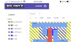
In the spirit of continuing the theme of El Cheapo chip design, we’re going to go super cheap now and look at a tool that lets you explore and perform silicon-level ASIC design on any machine, perhaps even a smartphone (shown in the image, above—I double-dog dare you to try to tape out a chip on your phone), because it runs on your web browser.
Even if you’re not designing a chip, it’s a fun doodling game, like scribbling on a notepad, to play during a boring meeting. So, let’s take a look at, and poke around in, “SiliWiz,” a polygon-level silicon chip editor designed by Tiny Tapeout cofounders Matt Venn and Uri Shaked, in this installment of Nonlinearities.
More in this Series
Chop and Channel on the Cheap
The first step in doing a polygon-level ASIC design is understanding what various device structures look like, whether they’re NMOS or PMOS transistors; interconnects like metals and vias and contacts and polysilicon; resistors; MIM capacitors; or basic n-diffusion and p-diffusion, and p-substrate and n-well, regions. These are covered in many texts and online resources, so there’s not much point in reiterating them here. But in the spirit of not spending money, you can study/review the basics on a site like the one here.
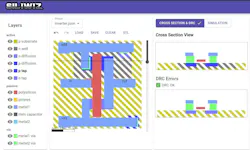
So, let’s dive right in and have a look at an NMOS and PMOS transistor, and a CMOS (“complementary,” meaning both P and N MOS transistors are in the circuit) inverter gate (Fig. 1). We’ll lift the figure right out of SiliWiz, using a bit of Photoshopping (actually GIMPing) to keep both MOSFET cross-sections in one illustration. Yeah, this silicon layout might be considered digital, but let’s pretend it’s just a high-gain amplifier with capacitors all over the place and keep our analog hats on.
To write this article, I’m using my small, light, gnarly-OS, work laptop and running SiliWiz on my “Big Dawg” gaming machine (which I have never played an actual game on—it’s my engineering rig, and, as a 17-in. laptop, the notion of it being portable at 9.74 lb. is a huge stretch of the imagination, though I do travel with it in its caster-wheeled roller bag when I think I need to run simulations or do CAD work away from home).
Big Dawg is complete overkill for this tool, though I did install the Open-Source ASIC design tools on it. One of those tools can generate a schematic from a (SiliWiz) SPICE netlist, and that toolset can be used in the flow toward an actual tapeout in a specific technology node.
SiliWiz comes with a few examples of circuits that are easily loaded with a pulldown selection from the “Preset” section of the landing page. Included are silicon layouts for a couple of capacitor types, a poly resistor, four MOS transistor types, and thar even be a “SkullFET” (no spoilers yet, so have a look) ya scurvy dogs.
On the left half of Figure 1 is the example layout of a CMOS inverter gate. To its immediate right, you can see a slider, with a fine line cutting across the layout—that line defines the cross section of the silicon being seen to the right of Figure 1.
With some GIMPing, I took two cross sections and added the lower one to the first screen cap image, the upper one being a PMOS transistor being cross sectioned and the lower cross section being an NMOS transistor. The legend on the left describes what each of the layout’s colors means and doubles as a selector for which layer is active for drawing a polygon (square or rectangle). Rule checking is performed real-time while drawing the polygon, and the results appear in the “DRC Errors” section of the page.
Let’s compare the SiliWiz inverter’s transistor cross sections to the cross section from the Weste and Harris textbook (Fig. 2).
Apart from a few seemingly sloppy layer stackups in SiliWiz, what’s in the textbook is what we see as transistor cross sections in the inverter layout. The exception is that the fictional silicon process being used has a p-type substrate as “bulk” and an n-well is created in the substrate to create equivalence (physicists would disagree, but engineers be like, “meh”) to the n-type bulk in the textbook. We may see this tool evolve to use a real PDK and be able to generate tapeout files in the future, though a commitment hasn’t been made yet to do so.
SiliWiz SPICEs Things Up
Spoiler alert: While you’re playing with this fancy ASIC engineer’s etch-a-sketch, there’s a bunch of stuff that’s been running in the background.
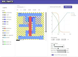
Clicking on the “Simulation” tab reveals the output plot of a SPICE simulation, where the parameters in the simulation are controlled, again in real-time, by sliders. The plot pane signal traces can be selected for display or deleted with simple and intuitive buttons in the “Plot signals:” section of the SiliWiz page.
I was curious and did math on two signals when placing another trace in the plot, and....it worked! The plot didn’t rescale to cover the negative magnitude, though. I've contacted the developers to see if they can quickly fix this oversight, if it is one. The plot traces, including my wacky subtraction of “input-output," are shown in Figure 3.
This was pretty spiffy, but if the “Show SPICE (advanced)” switch is toggled to “on,” if you scroll down (at least that’s the case with Big Dawg’s screen), you’ll see the extracted SPICE Code for your (inverter in this case) layout (Fig. 4).
The extracted SPICE file can be downloaded in its entirety for further use, including generating a schematic and a real tapeout layout in other tools that can do “back annotation” as part of an LVS (layout vs. schematic) function.
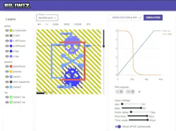
Make any changes to the plot signals, the parameter sliders, or...get this...THE LAYOUT… and you’ll observe that the extracted SPICE Code, and Tech File, is immediately updated and the simulation run continues to produce the plot plane output. This means you can play with polygon geometry and watch the electrical implications of doing so, all the while having DRC checks to make sure what you’re doing might actually be manufacturable. The “SkullFET”-based circuit of Figure 5?
Yeah, it passes DRC, which means it can be fabricated by falling within the rules of our fictional PDK. It’s a functional CMOS inverter gate as can be seen in the SPICE output plot!
There’s also an “Edit SPICE” switch where you can hand-edit the SPICE code and immediately see the result in the waveforms output. For example, I went in and changed the 5-V values to 3.3 V to see the effect on the circuit by running it on a lower supply voltage. Change it to 1.8 V and the output for the example layout gets a bit wobbly in the knees.
A Tool for the Trade (or a School Tool?)
So, if you have a standard cell design, a small function like a ring oscillator to try out, or are just bored, surf over to app.siliwiz.com and play around with a fun tool. It could be perfectly suited to exploring designs of small-scale-integration (SSI) devices or an inexpensive way for students to learn how CMOS transistors and passive components work.
If the developers someday do target an actual PDK and export the layout files, this would be an extremely inexpensive tool where students on a class PC can design and tape out a small chip function without having to install any tools on the PC.
The next blog entry in this series plans to cover another tool you can also use for fast and easy ASIC Design. It’s actually been used to tape out real chips.
Upcoming Blogs and Articles
Firstly, this design series on <$1,000 chip design is going to temporarily hibernate, but should reawake in the second week of December, since a couple of other time-critical things have crept in that I think are worth our time—yes, on AI.
But not AI hype. You should know me better than that by now. These should rock your inner nerd; my upcoming AI opinion blog should have you stroking your chins and then perhaps grabbing the torches and pitchforks to overthrow the tech tyrants.
Due to the timing of the coming-out of an analog computing startup that I’ve already hosted on video (currently with our video producer for editing), and a podcast on a somewhat controversial advanced technology that I think you’ll all enjoy, my next Nonlinearities blog entry will post a day later than its usual third Monday installment.
And speaking of interesting tech that you may not know much about, I’ve invited a few technical articles to be contributed by savvy practitioners to learn us [sic] all on things most of us don’t do in our day jobs, or perhaps we may include someday in our designs. If you consider yourself an expert in a certain area and would like to share some of your knowledge with practicing EEs worldwide in an Electronic Design contributed article, hit me up with an email, since it’s not easy for me to cross paths with some of you in order to invite you to contribute an article or two or three or.....six.
Yup...I’m now editing an invited six-part contributed article series on that old Bob Pease favorite, the K2-W vacuum tube op amp from 1952. It will start up this month and run weekly—I think it includes giving you just enough knowledge to play with designing with tubes and is spider-venom-level flex at the water cooler, or at the coffee station if you still work in an office. Not sure how much good it’ll do you in search of an S.O. at a bar or other venue as an opening line, though, or as a conversational topic on a date or over dinner with a spouse.
All for now,
-AndyT
Andy's Nonlinearities blog usually arrives the first and third Monday of every month. To make sure you don't miss the latest edition, new articles, or breaking news coverage, please subscribe to our Electronic Design Today newsletter.
Here are some related low-cost chip design articles we've hand-selected for you:
About the Author
Andy Turudic
Technology Editor, Electronic Design
Andy Turudic is a Technology Editor for Electronic Design Magazine, primarily covering Analog and Mixed-Signal circuits and devices and also is Editor of ED's bi-weekly Automotive Electronics newsletter.
He holds a Bachelor's in EE from the University of Windsor (Ontario Canada) and has been involved in electronics, semiconductors, and gearhead stuff, for a bit over a half century. Andy also enjoys teaching his engineerlings at Portland Community College as a part-time professor in their EET program.
"AndyT" brings his multidisciplinary engineering experience from companies that include National Semiconductor (now Texas Instruments), Altera (Intel), Agere, Zarlink, TriQuint,(now Qorvo), SW Bell (managing a research team at Bellcore, Bell Labs and Rockwell Science Center), Bell-Northern Research, and Northern Telecom.
After hours, when he's not working on the latest invention to add to his portfolio of 16 issued US patents, or on his DARPA Challenge drone entry, he's lending advice and experience to the electric vehicle conversion community from his mountain lair in the Pacific Northwet[sic].
AndyT's engineering blog, "Nonlinearities," publishes the 1st and 3rd Tuesday of each month. Andy's OpEd may appear at other times, with fair warning given by the Vu meter pic.
Voice Your Opinion!
To join the conversation, and become an exclusive member of Electronic Design, create an account today!

Leaders relevant to this article:


