Q&A: Taking a Closer Look at AMD’s High Bandwidth Memory
This file type includes high resolution graphics and schematics when applicable.
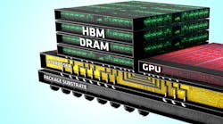
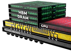
High Bandwidth Memory (HBM) stacks memory on the same chip as the CPU or GPU that uses it, instead of putting the memory off-chip (see “High-Density Storage”).
I talked with AMD’s Bryan Black about HBM. Bryan is a Senior Fellow at AMD who is responsible for all aspects of AMD's die-stacking technology effort.
Wong: I understand that work began on HBM about seven years ago. What was the initial driver for this effort?
Black: The initial effort was to develop die-stacking technology to bring together different system functions in a package, so the program started much broader than HBM. Memory, specifically DRAM, become interesting four to five years ago after we realized that the power-scaling of GDDR5 would not allow us to achieve the performance and energy-consumption targets required to lead in graphics. We looked at HBM as a new solution that would continue scaling for many years to come and help us achieve leadership in the market.
Wong: With complex technologies such as HBM, it often takes partnering with others to bring a finished product to market. Who did you partner with, and how was HBM developed?
Black: The DRAM is only part of the equation. Building the entire solution required contributions from a number of ecosystem partners in packaging, assembly, and test, as well as DRAM. AMD found highly capable partners to develop the fundamental technologies required to bring the final product to market. It required close collaboration with SK Hynix as the HBM vendor, UMC to make the interposer, and Amkor and ASE for interposer finish, packaging, and test. AMD was driving all of these vendors toward the goal of building the best graphics processor possible, with our GPU at the heart of the package.
Wong: Along the way there are always obstacles, technical or financial. What were the most significant you encountered, and how was it overcome?
Black: There was no single, overwhelming obstacle that consumed a majority of the effort or time. The challenge instead was the significant number of new technology components, combined with new business partners, and the sheer number of modifications required across every touch-point along the way. These were considerable, as there were over 400 different items on the project list, including business and technical challenges that had to be addressed to make the final product possible. There are the obvious new technical features like through-silicon vias (TSVs) and stacked DRAM, each with a unique set of issues. But there was also the job of creating the business model for a new way to build a silicon system and then establishing the entire ecosystem to make it happen.
Wong: It’s been some time since this effort started. Has the need for memory solutions like HBM changed over recent years?
Black: Along the way we discovered that the need for a new memory system was even greater than we originally predicted, meaning that the business case only grew stronger as time passed. For example, if you look at the first AMD product utilizing the technology, the Radeon R9 Fury X, we focused on driving super-high-resolution displays, virtual-reality experiences, and smooth gameplay. Those all require a lot of processing horsepower. In addition, we deliver this in very small form factors because the vertical stacking of memory takes up less space on the board. None of that would be possible without die stacking and HBM.
Wong: Is the market ready to adopt something so radically new?
Black: Enthusiast PC customers are the primary market for the R9 Fury X and they’re always looking for the latest and greatest, so the initial response has been fantastic. We are seeing clear indicators that the primary target market is clearly ready to embrace HBM, and hungry for the benefits it brings. For the more mainstream user, they probably don’t ever need to know that they have HBM and die stacking under the hood. It will just be there, chugging away, delivering excellent graphics and gaming as it was intended.
This file type includes high resolution graphics and schematics when applicable.
Wong: So far, HBM has only appeared in your high-end Fury X graphics cards. Do you see applications for HBM beyond GPUs at AMD?
Black: Absolutely. And again, it’s not just applications for HBM, but how we leverage all of the different die-stacking technologies that have been developed. As an example, we see obvious uses for die stacking in servers and high-performance computing. Die-stacking technology and HBM can improve virtually any market that would benefit from smaller, lower-power, higher-performance solutions.


