Undergrad EE Students Await Their Newborn TI-Fabbed Chip Designs
What you’ll learn:
- Georgia Tech’s new mixed-signal ASIC design course where teams of three undergrads and one “Chip Captain” grad student design a full-custom chip.
- Georgia Tech’s partnership with Texas Instruments, where TI supplies the PDK, live guest lecturers, and a fabrication service on its advanced 300-mm process.
- A podcast of an interview with Georgia Tech’s Dr. Shaolan Li regarding this novel course that accesses TI’s fab process and manufacturing.
- Georgia Tech’s course covers the design, simulation, layout, back annotation, tapeout, and testing validation of a custom ASIC over a span of two semesters, with a real chip being fabbed during summer break.
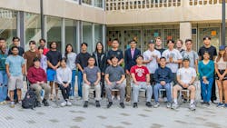
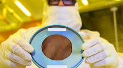
There’s excitement building among the cohort of 40 students, most of whom are pictured above, enrolled in the Dr Shaolan Li’s ECE 4804/8804 class at Georgia Tech’s School of Electrical and Computer Engineering (ECE). The anticipation is over fully-custom-designed semiconductor chips that are about to be delivered from their fabrication partner, Texas Instruments, after spending the better part of this past summer in TI’s 300-mm advanced fab in Richardson, Texas.
These aren’t garden-variety analog “jellybean” devices found in an electronics distributor’s catalog—they’re 10 fully unique chip designs, each having been a vague conception about nine months prior. Their baby is about to be born.
The Cohort Percentages are Mostly B.S.*
These 40 students are the first cohort in a new, two-semester course in Analog VLSI being taught by Dr. Li (Fig. 1) in collaboration with industrial partner, Texas instruments.

The first of the course’s two semesters began in January 2024, allegedly the “spring” semester. A 75% mix of mostly senior undergrads registered as ECE 4804, and 25% grad students registered as ECE 8804, would be taught how to design, simulate, layout, back annotate, and tapeout a fully functional Analog VLSI chip for fabrication by Texas Instruments during summer break.
Of the undergrads, about 30% are on a BS/MS “track,” which meshes well with their final semester during spring as bachelor’s candidates. The second semester of the course in the fall meshes with their first semester as master’s students.
TI’s involvement in the Georgia Tech partnership goes well beyond mere wafer fabrication and die packaging, though. The company also provided the school with its PDK (process development kit), which provides the rules and models that represent the available devices and fab process for the suite of CAE tools being used.
The “Artisan” toolset is based on Cadence Automation, including Virtuoso for design, Assura Physical Verification, Spectre simulation, along with MATLAB doing the heavy lifting on design verification and likely for simulation test vector generation.
Loose Lips Sink Chips
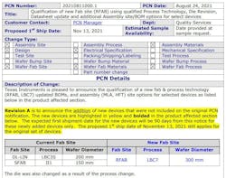
Dr. Li was annoyingly respectful of the terms of his NDA with TI and could not say much more than it being a 250-nm-ish BiCMOS process. Georgia Tech’s PR group stated in their press release that it was being fabbed in the new Texas 300-mm fab. TI’s PR team was also tight-lipped about any process details, after being asked for details—stuff engineers just want to know, not steal.
These information “challenges” led to this editor committing the act of journalism by looking up DigiKey’s process change notice for a recently qualified TI analog chip (Fig. 2). It appears that the undisclosed process may be TI’s LBC7 process running on 300-mm wafers in its newly expanded Richardson Fab, RFAB2. This is purely speculative, but it seems to fit nicely. It might be tweaked a bit, but doubtful with all of the legacy chips designed on LBC7 and TI claiming to run 100 million chips a day in the fab.
Further sleuthing on the LBC7 process assumption by looking at a somewhat obscure, peer-reviewed conference paper from two decades ago revealed the following information [this is all publicly available info, so the TI info gatekeepers were merely erring on the side of caution, and Dr. Li has a LOT more detail in his possession under NDA with the PDKs having non-public device models where correlated device performance can be extracted]:
“LBC7 combines a 0.25um analog CMOS technology modularly with LDMOS technology to create an advanced dense BiCMOS-DMOS power technology. It features state-of-the-art LDMOS devices rated from 7V up to 30V. Three flavors of LDMOS devices are supported for each voltage rating. In addition to the standard low side and high side devices, the technology also offers isolated drain LDMOS devices up to 30V rating [drool!]. Additionally, the process features dense 3.3V, 5V, 7V digital and analog CMOS, higher voltage drain extended (DE) n and p-channel devices, low Vt CMOS, depletion PMOS, bipolar devices, high voltage diodes and an assortment of passive devices. The process also features fully stackable triple level metal with fourth level as option and has thick CuNiPd for power routing and bonding on active silicon (BOA).”—Pendharkar et al (2004)1
An NDA is only as tight as the obligeds’ honor, and there are at least 80 eyeballs on the PDK, of which 4 to 10 might wind up in TI’s employ after this brilliantly strategic training/mentoring session on TI’s proprietary toolchain (with the rest being dispersed on the winds to competitors). So, it would make sense for the PDK to be truncated to include only “need to know” devices for executing the class assignment.
Some of those “secret sauce” TI power devices are drool-worthy as compared to what’s available in the Skywater analog/mixed-signal process. For example, maybe TI will open up a foundry someday for public MPW access on the cheap with an Open SDK for LBC7 so that we can design power devices using Open-Source tools. With CHIPS Act funding, it would be a nice goodwill gesture to U.S. residents that paid in the taxes for the act.
SARs and Masks
Despite the course being titled “Analog VLSI,” the assigned chip is optimistically MSI at around 500 transistors per chip, and is a mixed-signal design comprised of analog and digital circuits to form a SAR ADC with S/H (successive-approximation-registered architecture [Ed. note: I think it should be "SARA," but it’s stuck forever as "SAR" in a bazillion textbooks and in peer-reviewed papers where nobody questioned the awkward-sounding dangling participle] analog-to-digital converter with sample and hold).
The ADC spec is fairly loose due to semester time constraints, rookie chip designers, and to able to go easy on the three undergrads in the four-person-per-chip design team—the remaining person is “Chip Captain,” a grad student with more coursework, knowledge, and responsibility for chip functionality and whom will be graded more rigorously. Specifically, the spec is a 100-ksample/s SAR ADC, 10-bit architecture with 9 ENOB and a switched-capacitor S/H in the input of the signal path; a 5- × 5-mm die area is allocated per foursome.
Again, due to knowledge and time constraints, major topologies are supplied in the course materials put together by Dr. Li, which are comprehensive and on point. In fact, they’re so comprehensive that textbooks simply aren’t available to cover the details needed in executing a chip design from schematic to tapeout in one semester. Guest lecturers from Texas Instruments cover some of the course material, lending an industry-expert-mentoring atmosphere to the course versus being purely academic content.
“TI has a long history of university involvement, and Georgia Tech is one of the schools with which we’ve worked for many years. We believe it’s important for students to leave college with real-world experience in analog design and testing so they can enter the workforce better equipped to make an immediate impact. Having a TI engineer assist with curriculum development and guest lectures brings current industry experience into the classroom, supplementing the professor’s expertise and allowing students to learn about TI’s product development, fabrication and chip integration processes directly from an industry leader. We’re excited to see how this collaboration inspires and equips students.”—Roland Sperlich, Vice President, Texas Instruments
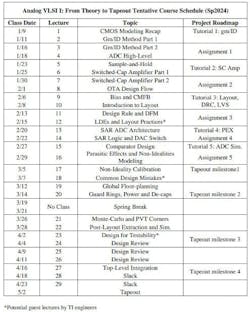
A course schedule, swiped off a publicly open server (Fig. 3), gives an indication how intense this class can be—this is a complete chip design in one semester while still studying and passing other courses for a BS or MS degree.
“Taking on this amount of work in such a short amount of time is challenging, but students are embracing it with enthusiasm. The experience not only enhances students’ understanding of the complexities involved in chip design and fabrication, but it also significantly reduces the ramp-up time once students enter the industry.”— Dr. Shaolan Li, Georgia Tech
With the chip laid out, back annotated, parasitics simulated, and the layout “taped out,” the 10 teams’ unique chip designs are placed on a reticule and sent off at the end of the spring semester to TI for mask generation and fabrication in its 300-mm Texas fab. For this first cohort, the tapeout occurred in August 2024, with packaged chips expected in hand by mid-October to early November.
Running some numbers through Silicon Edge’s chip estimator reveals about 2,446 die would be stepped on a 300-mm wafer, or 244 of each chip design for the cohort from just one wafer, ignoring process monitors.
Devices will be sorted according to their reticule mapping, so that each team gets their own chips to validate. Might be an idea to have a subsequent spring course for each team to design and build a 15×15 phased-array ultrasound receiver board with the remaining 243 chips...
“Bee”ing Patient
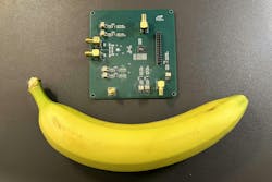
The 2024 fall semester had started, as did the second half of the course, despite the absence of fabricated and packaged ASICs from TI. Fortunately, Dr. Li had test chips fabricated and packaged from previous work on a different process that could stand-in as surrogates (Fig. 4). This would allow each team to begin the process of validation test setup and make practice measurements, so that they could hit the ground running when the UPS/FedEx delivery comes in.
[Ed note: We had once fabricated an urgent lot of GaAs devices for a customer in Asia only to have the cargo plane burn up completely at the destination, meaning a fab restart. Chip fab is very unpredictable, no matter how greased the process].
That sound of student’s drumming fingers on desks at a university in Georgia should be replaced by cheers in a month or so as the fully custom designed chips, by undergrad engineering students no less, are brought up and verified as functional.
Dr. Li hopes to acquire a wafer-probing ATE such that the testing of the student projects can be on-wafer. It makes a lot of sense in terms of shaving a few weeks off given the short timespan between tapeout at spring semester end and the start of the fall semester. If there’s one lying around, idle, donate it to the school for a tax deduction.
Much of the Georgia Tech information for this article was obtained in a somewhat lighthearted 22-minute Zoom call between Electronic Design’s Analog Editor, Andy Turudic, and Dr. Li. To listen to it as a podcast (it’s just audio that plays on any computer or smartphone just as a Youtube video does), click here.
*Bachelor of Science
Reference
1. Pendharkar, Pan, Tamura, Todd and Efland, "7 to 30V state-of-art power device implementation in 0.25μm LBC7 BiCMOS-DMOS process technology," 2004 Proceedings of the 16th International Symposium on Power Semiconductor Devices and ICs, Kitakyushu, Japan, 2004, pp. 419-422, doi: 10.1109/WCT.2004.240297.
Andy's Nonlinearities blog arrives the first and third Monday of every month. To make sure you don't miss the latest edition, new articles, or breaking news coverage, please subscribe to our Electronic Design Today newsletter.


About the Author

Andy Turudic
Technology Editor, Electronic Design
Andy Turudic is a Technology Editor for Electronic Design Magazine, primarily covering Analog and Mixed-Signal circuits and devices and also is Editor of ED's bi-weekly Automotive Electronics newsletter.
He holds a Bachelor's in EE from the University of Windsor (Ontario Canada) and has been involved in electronics, semiconductors, and gearhead stuff, for a bit over a half century. Andy also enjoys teaching his engineerlings at Portland Community College as a part-time professor in their EET program.
"AndyT" brings his multidisciplinary engineering experience from companies that include National Semiconductor (now Texas Instruments), Altera (Intel), Agere, Zarlink, TriQuint,(now Qorvo), SW Bell (managing a research team at Bellcore, Bell Labs and Rockwell Science Center), Bell-Northern Research, and Northern Telecom.
After hours, when he's not working on the latest invention to add to his portfolio of 16 issued US patents, or on his DARPA Challenge drone entry, he's lending advice and experience to the electric vehicle conversion community from his mountain lair in the Pacific Northwet[sic].
AndyT's engineering blog, "Nonlinearities," publishes the 1st and 3rd Tuesday of each month. Andy's OpEd may appear at other times, with fair warning given by the Vu meter pic. His cartoon series, "Inventors", appears each week in Electronic Design Weekly.
Comment About the Article
To join the conversation, and become an exclusive member of Electronic Design, create an account today!

Leaders relevant to this article: