How Emerging Ethernet Standards Will Propel Hyperscale Data Centers and ML Apps
What you’ll learn:
- A brief history of Ethernet standards.
- Current updates on the IEEE Std 802.3df and IEEE P802.3dj projects.
- Building blocks for next-generation, hyperscaled data centers.
Building on the original IEEE Std 802.3 standard first published in 1985, the IEEE Std 802.3df and IEEE P802.3dj projects represent the latest advances in Ethernet standardization. These new projects are paving the way for next-generation Ethernet, with aggregate link speeds of 200 Gb/s, 400 Gb/s, 800 Gb/s, and 1.6 Tb/s. Specifically engineered to address the needs of emerging hyperscale data centers and large-language-model (LLM) machine-learning (ML) applications, they promise to deliver significant improvements in performance and scalability.
These projects introduce innovations in media access control, management systems, and physical-layer specifications across both optical and electrical signaling technology. In optics, they leverage single-mode fiber signal modulation and detection technology to achieve performance metrics for physical media attachments (PMA) ranging from 500 m with PAM4 to 40 km with DP-16QAM. Their arrival represents a significant stride in optical technology, enhancing data-transmission capabilities over various distances.
A Look at the Last 802.3 Standards
On the electrical side, these projects establish a new foundation of 212-Gb/s interfaces designed to support everything from direct attach copper (CR) to chip-to-module (C2M), chip-to-chip (C2C), and backplane (KR) interfaces.
The most technical and engineering challenged electrical interface is the C2M interface, which is the principal physical-layer interface used in QSFP or OSFP module-based fiber configurations supporting the emergence of 104-Tb/s switching technology. This is a key building block in next-generation artificial intelligence and hyperscaled data centers, and central in the demand of next-gen 1.6-Tb/s copper and fiber-based interconnects.
>>Download the PDF of this article
A Brief History of IEEE Ethernet Standards
A quick look at recent and current IEEE projects is important to properly see what the future holds.
- IEEE Std 802.3ck-2022 specifies a 106-Gb/s per lane physical layer and management parameters for 100-, 200-, and 400-Gb/s aggregate interfaces.
- IEEE Std 802.3df-2024 specifies media access control and management parameters for 400 and 800 Gb/s, and physical layers through the reuse of existing 106-Gb/s per lane physical-layer capabilities.
- IEEE P802.3dj (estimated completion in 2025) specifies a 212-Gb/s per lane physical layer and media access control for 1.6 Tb/s and management parameters for 200-Gb/s, 400-Gb/s, 800-Gb/s and 1.6-Tb/s aggregate interfaces.
The IEEE P802.3dj project continues the IEEE Std 802.3 development cadence, in support of demands for higher speed and more efficient electrical and optical signaling.
This contribution will focus principally on the new 212-Gb/s physical-layer interface under development for IEEE P802.3dj. This new physical interface pushes the boundaries of electro-optic transmission systems, connectors, and SerDes designs (Fig. 1).
Several known channel parameters are built into IEEE P802.3dj today. Most notably is a channel profile starting with a die-bump test point (TP0d) at the transmitter and ending at the receiver die-bump test point (TP5d). The nominal loss between these two test points is 40 dB and a signaling Nyquist frequency of 53.125 GHz. Figure 1 illustrates a typical host model with TP1a as it would be evaluated for a C2M configuration and a TP2 test point as seen from the perspective of a passive cable.
IEEE P802.3dj Pushes Ethernet Bandwidth
IEEE P802.3dj incorporates an asymmetrical loss model to accommodate the architectural need for channel-loss optimization in the assorted C2M, CR, KR, and C2C configurations. Several host channel-loss configurations are in draft form, ranging from Host-Low loss of ~6 dB, Host-Nominal loss of ~11 dB, and Host-High loss profile of ~16 dB.
The combination of the SerDes package model, a host loss profile, and a host compliance test fixture deliver the loss profile to the first accessible test point: A location referred as TP2 in the CR cabled topology or similarly TP1a in the C2M topology. In C2M, this loss can be as high as 32 dB (Fig. 2).
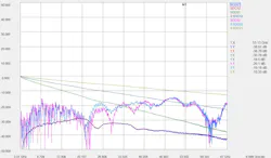
The insertion loss between the silicon TP0d and TP1a can range over the various allowable host loss profiles, which aren’t finalized at this time in the project. A net high loss profile of 32 dB serves as a unique case study for electrical validation challenges presented here. An illustration of these insertion losses and typical return loss parameters on test structures can be seen in Figure 2. The marker at 53.125 GHz indicates what’s typically the controlled insertion loss limit.
TP1a (Host output specifications) is where most electrical validation measurements are performed. These measurements include many of the familiar operations for signal noise distortion ratio (SNDR), steady-state transmitter voltage (Vf), and level separation mismatch ratio (RLM), which are present in IEEE P802.3dj’s (draft) Clause 176D (TP1a host output specifications).
IEEE P802.3dj has advanced efforts to harmonize the previously disparate validation methods existing between copper cable (CR) test validation at TP2 and C2M techniques at TP1a, which are effectively the same test point. For designers familiar with previous generations (53.125GBd PAM4) of C2M, the most noticeable change relates to the introduction of jitter specifications at IEEE P802.3dj’s TP1a test point.
The jitter specifications in IEEE P802.3dj are derived heavily from earlier clause 120D.3.1.8.1 techniques that examine a set of 12 strategic edges in a PRBS13Q (PAM4 PRBS13Q) test pattern to extract relevant jitter properties. The key jitter specifications used here include evaluating uncorrelated jitter (J4u) to a probability of 1:104, as well as non-compensable residual JRMS and Even Odd Jitter components referred to as EOJ.
Transmitting a fast edge test signal (5-ps transition times) through a 32-dB (at 53 GHz) combined package, host loss, and test adapter interface will perform significant low-pass filtering on the signal. The combined attenuation of this filtering and channel memory effects results in higher intersymbol interference (ISI) and lower edge slew rates for all of the single-, two-, and three-level transitions present in a PRBS13Q or PRBS9Q signal stream. The impact of these filtering impairments accounts for much of the observed differences between real-world measurements and simulation results.
Specifically, lower slew rates lead to larger jitter values since vertical noise creates jitter proportional to the magnitude of the noise divided by an edge’s slew rate. Meanwhile, increased ISI leads to more jitter variability between different edges. These effects aren’t symmetrical, though, as single-level edge transitions are the most highly impacted (highest jitter and highest variability), with moderate impact for two-level transitions and less impact for the three-level transitions.
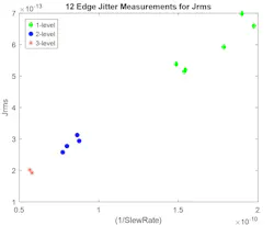
Figure 3 plots values of JRMS for the 12 chosen transitions in IEEE 802.3ck, which are a subset of the 8191 transitions in the PRBS13Q pattern. The three-level transition JRMS values are represented in red stars, while blue circles and green diamonds represent the two- and single-level, respectively.
The three-level transitions at the lower left extremity of this plot have the lowest JRMS values and the lowest variability, while the two- and single-level transitions that traverse higher (up and to the right) have higher JRMS values and more variability. This is an accurate illustration of what happens at the end of a high loss channel and is sometimes referred to as channel-induced jitter amplification. Because of this variability, the current process is to isolate jitter measurements to only the three-level transitions, which is where the notation of JRMS03 and EOJ03 has emerged.
Delving Further into IEEE 802.3dj
The latest proposal, IEEE 802.3dj D1.3, offers greater flexibility (Fig. 4). Jitter can be measured on any three-level transition. Results are reported using the rising and falling edges separately, which minimizes the jitter parameters. Moreover, the test can be performed using either a PRBS9Q or PRBS13Q pattern.
Figure 4 shows JRMS values for all three-level transitions in the PRBS13Q pattern, with the best rising and best falling results circled in black in the lower left corner. The intent of classifying jitter properties using JRMS03, and this latest proposal, focuses the attention on the transmitter properties while minimizing the high channel loss contributions to the highest extent possible.
A typical physical-layer jitter validation is illustrated in Figure 5. Jitter decomposition traditionally emphasizes all 12 of the available PAM4 transitions. For IEEE P802.3dj, the draft specifications focus on a limited set of rising 0 to 3 and falling 3 to 0 transitions (referred to as a three-level jitter specification). In this example, the J4U03 reported value is 95mUI (the greater of 3->0 or 0->3) against a nominal spec limit of 135mUI.
Figure 6 shows three-level transitions JRMS03 and EOJ03. Similar to how J4u reports the largest of either the rising or falling three-level jitter terms, this decomposition illustrates a JRMS03 maximum of 14.5mUI against a nominal limit of 23mUI and an EOJ03 of 21.9mUI against a nominal limit of 25mUI.
Many important changes are related to improved techniques and methods of measurement and signal characterization under development. Engineering and validation teams should be tracking these closely, and participating as a P802.3dj Task Force member is highly recommended.
Extending the IEEE Std 802.3 Legacy
The joint IEEE Std 802.3df and IEEE P802.3dj projects mark a watershed moment in Ethernet’s evolution, extending the legacy of the original IEEE Std 802.3 standard. As it continues to progress, these advances will play a fundamental role in supporting tomorrow’s high-speed, high-capacity networks, driving progress in data-intensive AI applications and shaping the future of Ethernet technology.
The Ethernet Alliance, the leading industry voice of Ethernet, champions the global advancement and adoption of Ethernet technologies. It remains committed to accelerating the deployment of IEEE standards by facilitating interoperability events that validate the latest technologies on real-world systems and interconnects.
Learn more about the Ethernet Alliance and how to get involved in shaping the future of Ethernet.
Acknowledgements to George Zimmerman (CME Consulting), David Rogers (EXFO), and David Gines (Keysight) for their contributions and assistance in producing this article.
>>Download the PDF of this article
About the Author

John Calvin
Member, Ethernet Alliance Board of Directors
John Calvin is a strategic planner and DataCom technology lead for Keysight Technologies. John has been bridging the measurement science gaps of emerging telecom and datacom development efforts for 20 years. He serves on the Ethernet Alliance board of directors and is a principal member in IEEE 802.3, OIF-CEI, InfiniBand, and PCIe development efforts.
John holds a BSEE from Washington State University, and his graduate level studies are in signal processing from Stanford University.
Voice Your Opinion!
To join the conversation, and become an exclusive member of Electronic Design, create an account today!

Leaders relevant to this article:


