What’s The Difference Between Silver Nanowire And ITO For Touchscreens?
Touchscreens have become one of the most intuitive interfaces in almost all consumer electronic devices. They’re popular in tablets, laptops, mobile phones, desktop monitors, kiosks, gaming machines, point-of-sale devices, automobiles, GPS systems, and more. The Windows 8 operating system has made them more popular in laptops, desktop monitors, and all-in-one computers. Most touchscreens use projected-capacitance technology and require high-quality transparent conductors to provide a rich user experience.
Related Articles
- New Materials Will Replace ITO To Improve Touchscreens
- Design A Lower-Cost Touchscreen System
- Design Touchscreen-Based Handheld Systems For Low Power Consumption
The incumbent technology for transparent conductors uses indium tin oxide (ITO).Indium is a byproduct of zinc mining that is sourced mainly from China. There have been supply shortages from time to time. ITO has played a major role in the growth of various electronic devices, particularly electronic displays and solar cells. To create a transparent conductor, ITO is sputter-coated onto a target substrate using a vapor deposition process in a vacuum chamber. The resultant coated substrate (usually glass) is chemically etched and patterned to form a transparent conductor that is used in touchscreens.
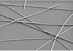
Cambrios’ ClearOhm coating material is an ink with silver nanowires (SNW) suspended within. The nanowires are made of crystalline silver with a diameter in the tens of nanometers and a length in tens of micrometers, giving it a high aspect ratio. When coated on a plastic (typically PET) substrate, the resultant film has a percolated network of highly conductive yet transparent silver nanowires (Fig. 1). The single crystal silver wires overlap, creating a network that is highly conductive since silver is the most conductive element on the planet.
Table Of Contents
• Requirements For Touchscreens
• Transmission Versus Conductivity
• Pattern Visibility, Haze, And Moireé
• Flexible, Bendable, Rollable, Touchscreens
The requirements for transparent conductors used in touchscreens vary by the touchscreen’s application and size. In general, they all require highly transmissive materials for good viewability, good conductivity to allow fast response to touch, and thinner materials so end products weigh less and are aesthetically pleasing. Most importantly, transparent conductors offer a lower cost of ownership to touchscreen makers and thereby a lower priced device for the consumer.
But these requirements are changing across most applications such as monitors, all-in-one computers, laptops, tablets, and mobile phones. Even higher conductivity below 100 Ω/square is sought so the touchscreens are more responsive to newer applications and a better user experience is realized.
For larger touchscreens used in applications such as 23-in. monitors, the higher conductivity is essential to offer fast response time with 10-finger touch capability. For mobile devices such as laptops, the need for thinner, lighter, and stronger touchscreens is driving the need for transparent conductors on film rather than traditional glass. As flexible displays become a reality, transparent conductors that can be conformed, bent, or even rolled to non-flat surfaces are part of the new requirements. Most importantly, as prices of consumer electronic devices continue to reach levels that cause mass adoption, the cost of the transparent conductors needs to keep pace.
Transmission Versus Conductivity
In touchscreen applications, particularly capacitive touchscreens for laptops and all-in-one computers, high transmission (over 90%) along with low resistance (less than 80 Ω/square) enable a 10-finger touch, which makes for a great user experience.
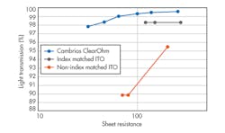
ITO on film is typically available at sheet resistances of more than 120 Ω/square. Below that range, ITO is typically available on glass rather than on film (Fig. 2). That’s primarily because the annealing temperature of a few hundred degrees centigrade for ITO is too high for plastic substrates, restricting its use to lower-conductivity films. ITO on glass, however, can be made for such applications. Higher conductivity is obtained by depositing a thicker layer of ITO on the glass substrate, though, reducing throughput since it consumes more time to deposit. Also, traditional glass substrates are heavy and thicker than film, which makes devices bulky.
OEMs increasingly prefer film-based transparent conductors. Commercially available index-matched ITO films have good transmission of over 98%, which makes them suitable for smaller diagonal size touchscreens like mobile phones where lower resistance is not mandatory (Fig. 2).
In case of the SNW transparent conductor, the material can be coated on film since the temperature needed to coat and dry it is around 100ºC, much lower than the softening temperatures of plastic films. Also, the production rate is the same regardless of the sheet resistance requirements. To obtain lower sheet resistance, a thicker coating of the exact same SNW ink at the same speed of coating (hence same throughput) is implemented. SNW has higher transmission than best-in-class ITO and offers well over 95% light transmission at sheet resistances significantly below what is achieved via film-based ITO.
Higher transmission means brighter display since the touch sensors do not impede light. Higher-transmission transparent conductors also mean longer battery life per charge in mobile devices.
Pattern Visibility, Haze, And Moireé
Both SNW and ITO technologies are strong in this area. Neither suffers from Moireé effects. The pattern visibility for ITO is not high compared to technologies such as metal mesh. Given the randomness of the silver nanowire distribution on film, this technology has almost no pattern visibility. Haze, on the other hand, is an issue with both technologies. Typical haze values for SNW on film and ITO on film are similar, with ITO on glass having a much better performance than ITO on film or SNW.
In this category, less is more. Transparent conductors that weigh less make consumer electronic devices like tablets and laptops more portable and rugged due to reduced mass. The reduction in thickness means designs are sleek and aesthetically more pleasing. In the case of touchscreens that require low sheet resistance below 100 Ω/square, the use of ITO on film is not possible. ITO then is usually deposited on glass, which makes the touch sensor on glass about 0.6 mm thick. In comparison, SNW on film is as low as 0.2 mm and as high as 0.4 mm. Similarly, traditional glass-based ITO sensors are significantly heavier than film-based SNW sensors. In general, SNW sensors on film are roughly 40% lighter and 40% thinner than their ITO counterparts.
Tablets, laptops, and LCD monitors of the past were heavier and thicker. Today the trend is to create truly portable devices and sleek all-in-one computers that demand thinner, lighter components. This is an area of advantage for film-based SNW sensors.
Flexible, Bendable, Rollable Touchscreens
Different display technologies and touchscreens have been pursuing flexible display applications for portability, ruggedness, and unique designs. In particular, organic LEDs (OLEDs) and e-paper are being targeted at new mobile applications. The touchscreens for these applications also need to be flexible, thin, light, and rugged.
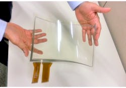
Imagine flexible mobile phones that are unbreakable. Imagine folding your 10-in. tablet so it fits in your pocket. Imagine rolling out a display from within your pen. Or, imagine notepad-size flexible displays or displays that wrap around a pillar or building. These types of products are becoming a reality. To enable these applications there is a need for flexible, bendable, rollable touchscreens (Fig. 3).ITO is a brittle ceramic material. It can be flexed slightly, but it’s likely to crack and become non-functional in bendable, transparent conductor applications.
SNW materials have been coated on flexible and rollable displays and tested by customers, successfully passing 100,000 turns around a 3-mm radius of bend. Film-based touch sensors using SNW transparent conductors are flexible, rugged, and already in use even on glass-based rigid display monitors, mobile phones, and all-in-one computers. For these applications, the flexible transparent conductor/touchscreens reduce the weight and thickness even though the host display itself is not flexible.
Silver is the best conductor of electricity on the planet and is roughly 100 times more conductive than ITO. From a material standpoint, a given touchscreen uses a lot less silver than indium. There are three areas for cost comparison: the infrastructure/equipment needed to coat the material onto a substrate, the cost of patterning the material, and the cost of the material stack that makes up the touchscreen.
The infrastructure needed to coat ITO requires vacuum deposition equipment that involves several million dollars of investment, and the application’s conductivity requirements influence throughput. For example, the throughput to coat a 50-Ω/square ITO layer is four times less than a 200-Ω/square ITO layer.
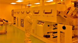
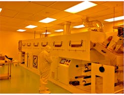
In contrast, SNW materials are solution-coated with significantly lower upfront investment in equipment such as pilot coaters (Fig. 4). The throughput/capacity of a given line does not vary with the conductivity/sheet resistance required for different applications. The roll-to-roll process employed to make SNW-coated material allows for expanding capacity very rapidly. The process is much more efficient. Also, the material utilization is better and does not suffer from the huge waste generated in the ITO deposition process.
Patterning costs for both SNW and ITO are the same if photo patterning or wet etch patterning methods are used. However, SNW has a cost advantage when the material is patterned using a room temperature laser process. The cost of laser patterning is roughly one-fourth the cost of photo patterning since the equipment costs are lower and there are no consumables like photo resist, etchants, or strippers. In addition, since the laser process does not use chemicals there are no waste disposal issues.
The throughput is high, and the quality of patterning is similar to the high-end photo process. The laser power required to pattern the SNW film is quite small and the quality of pattern is very high with excellent optical performance. Laser patterning on ITO could result in the substrate film being damaged since ITO requires more power or a longer duration to pattern, and the resultant patterned film could have pattern visibility that is objectionable.
Stack cost or per unit costs vary by stack configuration. Many more configurations are possible with SNW, and these configurations provide best-cost options for a given application. Some have fewer process steps (five steps versus 15 with traditional ITO) like in the case of SNW embedded in a dry film resist material. In other configurations like the one-film-solution (OFS), the stack does not use optically clear adhesives (OCAs), which further reduces cost. Overall, SNW-based touchscreens have shown to be slightly less to significantly less expensive than equivalent ITO film-based solutions.
ITO has enjoyed market dominance over several years since it is a well-proven technology that manufacturers understand. In some cases, manufacturers have already invested hundreds of millions of dollars in vapor deposition/sputtering equipment in well-depreciated factories.
The ITO process is well understood. The transmission is not better than SNW, nor can ITO film get to low sheet resistance, yet its performance is adequate for traditional applications for small diagonal size touchscreens. ITO is also very uniform, the pattern visibility is minimized, and the material is very stable.
SNW has an advantage over ITO in both transmission and low sheet resistance. The material is proven in several consumer products, manufacturing and per unit costs are lower, and scaling with SNW is much easier. The roll-to-roll processed SNW transparent conductor is a great choice for newer production facilities that need high throughput, easier processing, and material suited for flexible display touchscreens.
Rahul Gupta is the senior director of business development at Cambrios. Previously, he had more than 13 years of experience developing new technologies and products such as lasers for optical telecommunications at Lucent, full-color OLED displays and OLED lighting at Osram, and Generation 8 inkjet printing equipment for making color filters for LCDs at AKT (Applied Materials). He received his PhD from the University of California at Santa Barbara and an MBA from the Hass School of Business at the University of California at Berkeley.
Sriram Peruvemba serves as chief marketing officer for Cambrios’ worldwide operations. He manages the company’s global marketing, applications engineering, and business development efforts. He has more than 25 years of experience in the electronics industry. Prior to joining Cambrios, he served as CMO for E Ink Holdings, where he oversaw global marketing efforts for its e-paper and LCD businesses. He has also held senior level positions at Sharp Corp., Planar Systems, and TFS Inc. He serves as executive advisor to YFYJupiter as well.
