Prioritize Circuit Protection for USB Type-C Interfaces
This file type includes high-resolution graphics and schematics when applicable.
The USB Type-C connector specification and the related USB 3.1 and USB Power Delivery (USB PD) specifications promise to change the architecture of applications ranging from smartphones to laptops, and potentially many other devices. The USB Type-C form factor is reversible, so it’s much easier to use than its predecessors. However, for that glittering future to be fully realized, the new connector must be as robust and failsafe as the earlier USB Type-A and Type-B connectors.
One potential issue is that the USB Type-C is much smaller than USB Type-A. A USB Type-C connector has 24 pins with a 0.5-mm pitch, compared to the Type-A’s four pins with 2.5-mm pitch. The Type-C pitch increases the likelihood of a pin-to-pin short if the connector is inserted at an angle, or if debris becomes caught in the connector.
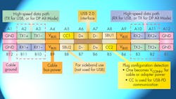
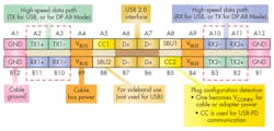
The problem is made worse by the number of substandard products that were rushed to market to take advantage of the USB Type-C phenomenon. Many of the cables don’t use the precision machinery and premium materials required to ensure reliable pin contact and long-term performance. Other cables have the incorrect VBUS pull-up resistor; thus, the power source will select the wrong voltage or the device will try to draw too much current.Figure 1 shows the USB Type-C pinout. Pin-to-pin shorts involving VBUS are particularly problematic if the host and device support the USB PD specification, because the VBUS pin can deliver up to 20 V and 5 A for 100-W fast charging power delivery. The configuration channel (CC) and sideband use (SBU) pins are directly adjacent to the VBUS pins. But USB is a 5-V system, so a short to VBUS could damage or destroy the interface components connected to the SBU and CC pins.
In response, last March, Amazon banned the sale of USB Type-C cables that didn’t fully comply with the Type-C specification issued by the USB Implementers Forum (USB IF), USB’s controlling body. Amazon’s action may remove one source of substandard cables, but dangers remain: Adding proper circuit protection to a USB Type-C design reduces the risk of system damage and field failures.
USB Type-C Protection Circuit Requirements
The protection circuitry for a USB Type-C application must handle two fault conditions: Protect adjacent pins against a short to VBUS, which could potentially put 20 V or more on the CC or SBU pins; and protect pins against electrostatic-discharge (ESD) events.
Let us examine these two conditions in more detail.
Short-to-VBUS Event
There are two possibilities for the short-to-VBUS event—short-to-VBUS through a cable and short-to-VBUS without a cable. If a short occurs in a Type-C connector that’s plugged into a device sinking VBUS power, the length of the cable separates the shorted CC or SBU line and the VBUS voltage source. If a Type-C cable is present, but the short occurs at the connector where VBUS is sourcing power, then the voltage source is applied directly to the CC and SBU pins, bypassing the cable.
Both short-to-VBUS use cases present challenges and need to be accounted for to ensure robust protection for the system.
During a short-to-VBUS sink event, cable inductance can generate ringing with a peak voltage up to double that of the steady-state final voltage. For a 22-V short, up to 44 V can appear on the SBU or CC lines during a short-to-VBUS event, and the protection circuitry must handle this voltage level.
A short-to-VBUS source event is challenging for a different reason. The inductance is very low without a cable, so the rise time of the short event can be less than 10 ns. Not only does this cause problems with parasitic capacitances in the OVP FET, the total resistance of the path is so low that the amount of current introduced on the CC and SBU lines can be substantially higher than with a cable.
ESD Event
Since the USB port can be accessed directly by the user, it must be protected against ESD. The relevant specification is the International Electrotechnical Commission (IEC) 61000-4-2 standard for ESD protection. This standard describes the required levels of protection from likely ESD events.
The situation is more challenging for the CC and SBU lines because, in addition to ESD, the protection circuitry must also take into account the possibility of a VBUS short that could place a sustained voltage of 22 V on the line. The ESD diode must have a trigger voltage above this level.
Most ESD diodes with a high trigger voltage also have a deep snapback characteristic and clamp to a very low voltage. The 44-V ringing induced by a VBUS short at the end of a cable can cause such a diode to conduct indefinitely, resulting in overheating and permanent damage.
A non-snapback diode must therefore be used. Unfortunately, there’s a shortage of such devices available on the market.
Discrete Design for USB Type-C Protection
If the designer decides to implement a protection solution with discrete components, what are some of the design considerations?
A FET placed in series with the CC or SBU line can perform overvoltage protection (OVP). The OVP FET must tolerate the 44-V ringing voltage that occurs with a VBUS short through a Type-C cable, but that’s not all. As we’ve seen, a direct short to VBUS has a 20-ns rise time, so the parasitic capacitances across the inline FET (CDG and CGS) will effectively create a short between the gate and the source, thus exposing the downstream USB PD controller to damage. This requires a clamping diode after the OVP FET and before the controller.
To keep an n-channel FET fully ON, the gate voltage must be kept 1.5 V or 2 V above the source voltage. With 5-V signals on the CC and SBU pins, the VGS of their inline OVP FETs have to be maintained at 7 V, requiring the addition of charge-pump circuitry. A p-channel FET doesn’t require a charge pump, but a control circuit will still be needed to ensure proper operation.
The USB Type-C specification also specifies that the CC pins must also be able to deliver up 1 W to power the circuitry in the active cable. To supply 4.75 V at 200 mA from a 5-V supply, the total allowable resistance in the CC line must be a maximum of 1.25 Ω, including the OVP FET and all other components. Minimizing the FET on-resistance increases its die size and hence cost.
Protection against ESD requires an additional clamping diode located at the connector, bringing with it the design issues we discussed in the last section.
Handling a Dead-Battery Condition
An additional complication arises when the battery in a USB Type-C device is completely discharged, i.e., during a dead-battery condition. The USB PD specification states that if a device has a dead battery, it will present a pull-down resistor RD to ground on the CC lines when it’s plugged in. After the charging port detects the dead-battery condition, it applies higher voltage to the USB port to charge the battery. The USB PD controller normally includes the circuitry to perform this function, but without power, the inline OVP FET is automatically OFF.
Because the USB PD controller dead-battery resistors are now disconnected from the Type-C connector, the designer must provide additional circuitry located between the OVP FET and the connector to perform this function. This circuitry must also disconnect the RD resistors when the dead-battery condition is no longer applicable.
Summing up, any protection solution must support the following conditions:
• Handle ringing up to 44 V for a VBUS short through a cable.
• Support <10-ns rise times on the direct short-to-VBUS event.
• Support IEC 61000-4-2 system-level ESD protection.
• Support a power capability of at least 5 V/W for Type-C ports that support active cable.
• Support the dead-battery condition for mobile devices that rely on Type-C as their power source.
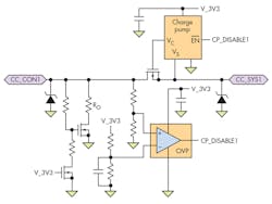
A discrete solution requires many components to satisfy this long list of requirements. Figure 2 shows an example of a discrete design for one of the four lines that must be protected. It contains three FETs, two diodes, a comparator, a charge pump, and assorted resistors and capacitors—a total of 17 components.
The comparator compares the voltage on the CC line to a reference. Under normal conditions, the charge pump is active, and the OVP FET is ON. If an overvoltage condition appears on the line, the comparator changes state and disables the charge pump, shutting off the OVP FET.
The two control FETs handle the dead-battery condition. If the battery is dead, the V_3V3 signal is low. When the charging port raises the CC_CON1 line high, the RD FET turns on and connects RD to ground. Once the V_3V3 signal goes high, signifying that system power is available for normal USB PD negotiation, the control FET turns on and turns off the RD FET, which disconnects RD from the CC_CON1 line.
Integrated USB Type-C Protection Solution
A better option is to incorporate the protection components needed for multiple lines into a single device. An integrated solution simplifies the design and saves board space.
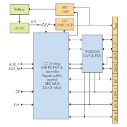
Figure 3 illustrates how the TPD8S300 USB Type-C Port Protector can perform the needed protection functions. The USB PD PHY and PD controller can be a device such as TI’s TPS65982.
The TPD8S300 inserts high-voltage FETs in series with the SBU and CC lines. When a voltage above the OVP threshold (typically 6 V) is detected on these lines, the high-voltage FETs open and isolate the rest of the system from the high-voltage condition.
The device also integrates eight channels of IEC 61000-4-2 ESD protection for the low-speed USB Type-C pins: CC1, CC2, SBU1, SBU2, and two D+/D- pairs. This removes the need for high-voltage transient-voltage-suppression (TVS) diodes at the connector.
The TPD8S300 is able to supply 600 mA over the CC pins when they’re configured to supply power. This power level is more than sufficient to power the Type-C cable; it can also supply the higher levels needed when operating in one of the alternate modes defined in the USB PD specification. On top of that, it integrates the high-voltage, dead-battery RD pull-down resistors to implement dead-battery charging simultaneously with high-voltage OVP protection.
An evaluation module (EVM) is available to assess the operation and performance of the TPD8S300. The EVM consists of the TPD8S300 mounted on a USB Type-C pass-through board, which enables users to test the operation of the device’s OVP and ESD protection features in their own systems.
Conclusion
The USB Type-C specification, in conjunction with USB 3.1 and USB PD, dramatically expands the scope of USB to include a range of power-charging functions. The combination of a small connector size and high power, though, poses significant challenges for the design of the protection circuitry.
Although a discrete design is possible, an integrated solution is a superior choice: It reduces component count, shortens the development cycle, and allows the designer to satisfy both OVP and ESD protection requirements in a compact package.
About the Author
Paul Pickering
Paul Pickering has over 35 years of engineering and marketing experience, including stints in automotive electronics, precision analog, power semiconductors, flight simulation and robotics. Originally from the North-East of England, he has lived and worked in Europe, the US, and Japan. He has a B.Sc. (Hons) in Physics & Electronics from Royal Holloway College, University of London, and has done graduate work at Tulsa University. In his spare time, he plays and teaches the guitar in the Phoenix, Ariz. area
Voice Your Opinion!
To join the conversation, and become an exclusive member of Electronic Design, create an account today!

Leaders relevant to this article:


