Nonvolatile storage is invaluable for all types of computing especially for embedded applications. Flash technology has dominated to date (see “The Fundamentals Of Flash Memory Storage”) but other technologies like FRAM (see “Low Power Microcontroller Has Up To 128 Kbytes Of FRAM”) and MRAM (see “Moving Back To Magnetic Storage”) have moved from research to deployment.
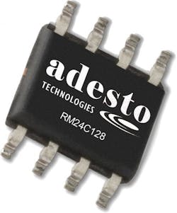
Resistive RAM, or ReRAM, is another nonvolatile storage technology. Conductive Bridging RAM (CBRAM) from Adesto Technologies is now being deployed. I talked with Narbeh Derhacobian,co-founder, president and CEO of Adesto Technologies, about CBRAM.
Wong: What is CBRAM?
Derhacobian: Conductive Bridging RAM (CBRAM) is a breakthrough technology platform that overcomes a critical power barrier to widespread innovation. CBRAM technology is universally adaptable as the underlying memory for a broad range of applications—from medical devices and appliances to wearables and smartphones. It enables 100 times less energy consumption than today’s leading memory technologies without sacrificing performance and reliability.
Wong: How does it work?
Derhacobian: To develop CBRAM, our Adesto team took a huge departure from traditional chip making. Most non-volatile memory technologies work using charged electron gates to store data. CBRAM uses a fundamentally different process, rethinking the most basic building blocks of computing.
Seven years ago, Prof. Michael Kozicki, a professor at Arizona State University’s electrical engineering department, developed a new method of storing information that showed exciting potential as a memory technology. The technology that was developed at ASU was called Programmable Metallization Cell or PMC. This technology is part of a family of emerging memory cell concepts known as Resistive Random Access Memory (ReRAM). ReRAM cells work on the principle of reversible switching of certain high resistivity dielectrics between a conductive and a more resistive state under suitable bias conditions.
The basic principle of operation CBRAM is based on a reversible creation of an electrochemically induced nanoscale conductive link in a special dielectric acting as an ionic conductor. The data in the memory cells are stored in form of the resistance value of the dielectric. High resistance implies logic data “0” and low resistance implies logic data “1”. The cells can be switched back and forth between these two resistance values upon application of a short voltage pulse across them. Adesto has implemented this technology in a standard silicon integrated circuit manufacturing line as the building blocks of its memory solutions.
This file type includes high resolution graphics and schematics when applicable.
The process of writing “1” and “0”s in CBRAM cells is very fast (10’s to 100’s of nanoseconds), but most importantly, it uses a far smaller amount of power than other nonvolatile semiconductor technologies. CBRAM cells can operate at sub 1V with currents in the microamp range and hence only requiring 10 to 100 times less energy than today’s flash memory solutions.
We at Adesto have spent seven years developing CBRAM for commercial applications and bringing it to market. Unlike other memory 'breakthroughs,' CBRAM production is up and running; the company has shipped over 1 million functioning units, and can demonstrate the technology's exceptional speed and performance even at ultra-low levels of power.
Wong: How does it compare to other non-volatile technologies?
Derhacobian: CBRAM approaches volatile RAM technologies in terms of speed, and far outstrips other NVM in speed and performance. And its power consumption is far, far lower than any existing technologies; Flash’s write energy per bit is 100 times that of CBRAM. Furthermore, CBRAM technology can be integrated in standard logic chip manufacturing processes making it an ideal solution for “embedded memory” solution in highly integrated System-on-Chip and microcontroller devices.
Wong: Are there particular application areas where this technology excels?
CBRAM is universally adaptable as the underlying memory across a broad range of functions and applications. This includes the broader memory markets that we all know today. However, our mission is not to be yet another commodity memory supplier. We work with customers to develop application-specific memory solutions. What this means is that we take a look at the end application and listen to how our customers are intending to use memory in their systems. Then we craft a more application-centric solution for them based on the proprietary solutions at our disposal. We have internal processes based on several key metrics (i.e. market size, pricing, development cost, etc.) that help us make a decision to develop these solutions. Although we see big potential for CBRAM in a range of industries and markets, currently we are focused on applications where low power is far more important than high density.
The most exciting is the emerging ‘Internet of Things’ industry. We see ourselves quickly moving to a world of electronics that will increasingly include an entirely new class of connected, data-centric applications where digital information moves fluidly across ordinary objects in our daily lives like appliances, cars, bridges, medical devices, and even human bodies.
Without low power consumption, the vision for 'Things' with embedded intelligence can't be realized, and we believe CBRAM is perfectly suited to enable this new era of innovation (projected by Gartner to include 30 billion connected devices by 2020).
Additionally, the emerging wearables industry holds huge promise for us. Specifically, CBRAM’s technology makes it ideally suited for data-enabled medical devices. The medical industry is making huge strides in innovating ‘intelligent’ medical devices and equipment (those that can gather, store, and transmit data), but there’s one huge problem: they cannot be sterilized using industry-standard processes, as these processes destroy the data-integrity of the content of flash memory today. CBRAM, on the other hand, can withstand e-beam and radiation sterilization processes at much higher doses than needed to sterilize medical equipment without any loss of functionality. We are currently talking to several leading suppliers in this area to offer unique and differentiated solutions in this exciting and emerging market.
Wong: How is CBRAM typically integrated into a system?
Derhacobian: We work with customers to build application-specific solutions depending on their needs. CBRAM integrates easily into existing manufacturing processes, and is flexible across a wide range of applications. CBRAM technology can scale long into the future regardless of the size, power or application needs.
Narbeh Derhacobian is the co-founder, president and CEO of Adesto Technologies. He has over 17 years of industry experience working on discrete and embedded memory technologies and more than 40 granted patents in various areas of semiconductor memories. Narbeh has held technical and managerial roles at SST, AMD, Virage Logic and Cswitch Corporations. His industrial experiences cover development and commercialization of split-gate NOR flash, ETOX NOR and NAND flash as well as SONOS based MirrorBit NOR flash technologies. Narbeh has a PhD in Solid State Physics from UCLA and an MBA from San Jose State University.


