High-performance network systems tend to be the playground of the big boys—companies like Cisco, with the staff to tackle the latest hardware as soon as it is available. The high end used to be 10 Gbit/s Ethernet but the cutting edge has move to 100 Gbit/s. Still, the 10 Gbit/s arena is still hot, and these days more workstations and PCs are still sporting 1-Gbit/s Ethernet links.
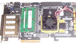
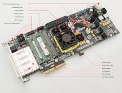
This made Digilent's NetFPGA-SUME (Fig. 1) board an interesting platform to check out. The system can handle 100 Gbit/s of throughput, and multiple boards can handle even more data together. The fastest link on the board is 10 Gbit/s. This is the same board I mentioned in a recent Lab Bench blog.
I will say up front that I have not really had a chance to exercise the board as extensively as I would like, simply because of the level of sophistication and the amount of time I have available—not to mention, the level of expertise required to really give this board a run for its money.
What I did do was take advantage of software available at NetFPGA.org. This is an open hardware and software site designed to support the NetFPGA boards. The Net-FPGA-SUME is at the top end of the family of boards addressed by the site. The platform is supported by vendors including Xilinx, Cypress Semiconductor, Micron, and Linear Technology.
It is also supported by a number of groups and educational institutions, among them the Computer Measurement Laboratory, the Engineering and Physical Sciences Research Council, the National Science Foundation, Stanford University, and the University of Cambridge. Some of the projects target network communication, but that is not the only thing the platforms can be used for. The boards can also be employed for data acquisition and high speed processing.
Digilent's NetFPGA-SUME hosts a Xilinx Virtex-7 690T supporting 30 13.1 GHz, RocketIO GTH transceivers—including four for 4 SFP+ interfaces, 10 on an HPC FMC connector, and eight on a QTH connector. There is also a PCI Express Gen 3 x8 interface. FPGA configuration memory consists of a pair of 512 Mbit Micron StrataFlash chips, three x36 72Mbits QDR II SRAM from Cypress Semiconductor, and a pair of 4 Gbyte DDR3 SODIMMs. The system has a Micro-USB JTAG connector that can double as a UART interface for debugging. The board also has a pair of SATA 3 ports.
The free version of Xilinx’s Vivado development platform is sufficient for getting started, but the full version (along with 10 Gbit/s transceiver IP) will be required to utilize much of the software on the NetFPGA Github site. I found the site easy to navigate, which is important because all the documentation and software are online. The box with the board only includes a USB cable.
The board can be plugged into a PCI Express site. This is especially useful if the PCI Express interface will be used in an application. The board can also sit on the workbench with an external power supply.
The NetFPGA-SUME is $9,750, but there is a considerable educational discount. There are many less-expensive and less-powerful platforms that may be more suitable. There are many applications that can get by with 1 Gbit/s links instead of 10 Gbit/s. I know I was hard pressed to come up with stuff in my lab, although you may have some 10 Gbit/s Ethernet ports handy.
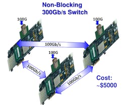
Given the expense and the expertise necessary to use this board, it is definitely not in the same realm as a Raspberry Pi or even a Xeon Phi. This is high-performance FPGA territory. It can do some amazing things with the right design handling 100 Gbit/s of data in real time. Many of the projects address things like software defined networking (SDN), including support for Openflow and image and video stream processing. Multiple boards could be linked together to provide a 300 Gbit/s non-blocking switch (Fig. 2).
Overall, it was an interesting exercise. The platform is great if you have interests that match projects on the NetFPGA site and are not interested in doing all the heavy lifting to get started. There are projects that are ongoing at the educational institutions.
About the Author
William G. Wong
Senior Content Director - Electronic Design and Microwaves & RF
I am Editor of Electronic Design focusing on embedded, software, and systems. As Senior Content Director, I also manage Microwaves & RF and I work with a great team of editors to provide engineers, programmers, developers and technical managers with interesting and useful articles and videos on a regular basis. Check out our free newsletters to see the latest content.
You can send press releases for new products for possible coverage on the website. I am also interested in receiving contributed articles for publishing on our website. Use our template and send to me along with a signed release form.
Check out my blog, AltEmbedded on Electronic Design, as well as his latest articles on this site that are listed below.
You can visit my social media via these links:
- AltEmbedded on Electronic Design
- Bill Wong on Facebook
- @AltEmbedded on Twitter
- Bill Wong on LinkedIn
I earned a Bachelor of Electrical Engineering at the Georgia Institute of Technology and a Masters in Computer Science from Rutgers University. I still do a bit of programming using everything from C and C++ to Rust and Ada/SPARK. I do a bit of PHP programming for Drupal websites. I have posted a few Drupal modules.
I still get a hand on software and electronic hardware. Some of this can be found on our Kit Close-Up video series. You can also see me on many of our TechXchange Talk videos. I am interested in a range of projects from robotics to artificial intelligence.


