What’s the Difference Between OTFT and Amorphous-Silicon Transistors?
What you’ll learn:
- OTFTs vs. a-Si transistors: Characteristics and performance.
- OTFTs vs. a-Si transistors: Mobility, stability, and uniformity.
- OTFTs vs. a-Si Transistors: Manufacturing process.
- OTFT applications go beyond traditional displays.
Thin-film transistors (TFTs) have become a key element in large-area electronics such as LCDs and displays. They enable higher resolution and contrast—without sacrificing refresh rate—through the control of individual pixels.
Following the invention of the transistor in 1947, the earliest TFT iterations were proposed and created in the late 1950s and early 1960s. They were built using a variety of materials, such as cadmium and indium, and they had varying performance and applications. However, these TFTs could only perform reliably across small areas and were therefore unsuitable for larger display sizes, such as monitors or televisions.
Further research led to the development of amorphous-silicon (a-Si) TFTs. a-Si proved to be reliable across larger areas, leading to the development of TFT-LCDs for commercial products. Following the commercialization of a-Si TFT, other types of inorganic TFTs, most notably low temperature polysilicon (LTPS) and oxide TFTs, were commercialized and are now widely used in OLED and smartphone displays. Today, a-Si-based TFT-LCD technology is used in billions of devices due to its relatively simple and low-cost manufacturing process for glass.
More recently, breakthroughs have been made in the development and mass production of organic thin-film transistors (OTFTs). Built using organic polymers that can offer the same or better performance as a-Si, they can be used in flexible, glass-free displays and other optics applications.
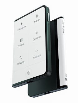
After years in development, the first OTFT entered commercial production in a mass-produced consumer product in June 2024—a cryptocurrency wallet from Ledger—with an ePaper display that wraps around a 180-degree exterior bend having a 3-mm radius of curvature. This milestone paves the way for increased adoption of OTFT-based components in future products (Fig. 1).
So, what are the main differences between a-Si transistors and OTFTs, and when might each be more suitable for a given product? Let’s look at the characteristics and performance of each and their manufacturing processes.
OTFTs vs. a-Si Transistors: Characteristics and Performance
Size, weight, and durability are important considerations in any electronic application. While thin-film transistors of all types are, as the name suggests, very thin and therefore light, they must be built onto a substrate. For inorganic TFTs, that usually means a glass substrate, which contributes nearly all of the thickness and weight to the transistor array, as well as limiting flexibility and robustness.
In recent years, we’ve seen growth in the commercialization of inorganic TFTs on polyimide substrates, most notably LTPS for thin or flexible OLED displays. Since inorganic TFTs, by their nature, contain ceramic/brittle materials, they’re prone to cracking if too much strain is applied. Hence, their use in flexible (OLED) displays requires careful design to ensure that the brittle layers in the transistor are at or very close to the neutral axis.
>>Check out this TechXchange for similar articles and videos
OTFTs, on the other hand, don’t contain any brittle/ceramic materials because all of the layers that constitute the transistor—the semiconductor and dielectrics—are made of plastics and, by their nature, are soft and can be strained to a very high degree without affecting performance (and certainly not cracking).
By default, they’re by default manufacturable on low-cost plastic films, and the resulting flexible transistors can be incorporated into flexible displays without needing to place the TFTs near the neutral axis. This opens up a high degree of product design freedom beyond what’s possible with silicon (Fig. 2).
Mobility, Stability, and Uniformity
Mobility is a key measure of electrical performance. In the world of displays, a higher mobility means a smaller transistor can be used, reducing its footprint and, therefore, increasing the pixel size, along with other benefits.
a-Si has been dominant for displays as its mobility is sufficient for many use cases, such as LCD TVs, monitors, and laptops (for very high PPI applications like smartphone displays, LTPS is often used). The mobility of a-Si is typically around 0.5 cm2/Vs—a far cry from the mobilities of silicon wafers used for microchips. However, this mobility can be achieved uniformly over very large areas; for example, across a 3- × 3-m piece of display glass.
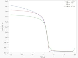
When organic TFTs were first in development, their mobility was orders of magnitude lower than a-Si and, therefore, not useful for driving display pixels. However, continual advances in polymer chemistry have realized organic materials and OTFT architectures with a mobility that’s equal to or better than a-Si. Today, FlexEnable’s FlexiOM OTFT materials, which are the first to be commercialized, surpass the mobility of a-Si by around a factor of three (Fig. 3).
OTFTs today also exhibit higher levels of Vt stability compared to a-Si, and they have Vt uniformity over large areas similar to a-Si levels—with 2% to 3% typical variation seen over large areas (FPD mother plates). That’s because solution-processed polymer organic semiconductors are particularly well-suited to forming amorphous films over large areas, compared to organic small molecule solution-processed semiconductors. This can often form polycrystalline films that result in poor uniformity due to mobility variation caused by grain boundaries.
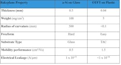
Collectively, these electrical parameters of FlexEnable’s OTFT platform all meet or exceed those of a-Si, meaning that the same electrical performance can be achieved on plastic as on glass (Fig. 4).
Comparing the Manufacturing Process for a-Si and OTFT
One key advantage of OTFTs is that they can be manufactured at very low temperatures. FlexEnable’s approach, for example, enables the manufacture of OTFTs at temperatures under 100°C for each step in the process. Not only does this low temperature allow for OTFTs to be built onto flexible bioplastic substrates (such as tri-acetyl cellulose, or TAC) instead of glass, but also results saves on energy consumption: approximately half the energy is saved in TFT production by switching from silicon to organic.
In comparison, silicon and other inorganic transistors necessitate high-temperature processes—even LTPS requires 450°C+ processes. Thus, it’s not possible to manufacture silicon TFTs on TAC substrates. Furthermore, each transistor device substrate will require many tens of such temperature cycles during manufacture, which consumes a huge amount of energy.
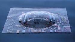
OTFT-based LCD displays (OLCDs) are designed to be built in existing display factories using standard FPD equipment. FlexEnable’s method is to attach the low-cost plastic film to the glass and then use a low-temperature process and FlexiOM OTFT materials to manufacture flexible organic transistors on the plastic film. It eliminates the need for energy-intensive steps such as high-temperature annealing and curing chemical vapor deposition (CVD), ion implantation, and sputtering.
Once the array is fabricated, LCD cell assembly is also done using conventional equipment. After assembly, the completed stack is removed from the carrier glass by heating, causing the TAC film to delaminate from the glass. This simple release process can be scaled to very large sizes. Importantly, the carrier glass does not form part of the BOM; it’s instead returned to the front of the line, cleaned, and laminated with a new TAC film for the next production run (Fig. 5).
For a-Si, these process steps are performed directly on the glass itself, which also becomes the substrate for the display, resulting in a flat glass LCD panel.
OTFT Applications Go Beyond Traditional Displays
While a-Si on glass is a suitable choice for many applications—primarily displays, but also some types of large area sensors (e.g., X-ray sensors)—it brings constraints in both mechanical and electrical performance depending on the use case and requirements. OTFTs offer unique advantages that expand their potential applications beyond traditional displays. What follows are a couple of examples of how OTFTs in production today can be applied to optical and display products:
Flexible Displays
OTFTs are in mass production in the form of a curved E Ink display for the Ledger Stax cryptocurrency wallet. Using OTFTs has enabled a curve radius of 3 mm and created a unique form factor and interaction method within the industry.
The flexibility of OTFTs allows for cutting-edge designs and new functionality that’s not possible with flat-panel displays. Apart from ePaper displays, this technology can also drive LCDs. The so-called organic LCD (OLCD) can be curved to conform to almost any surface and could even feature apertures or cutouts to, for instance, wrap around buttons. OLCDs are well-suited for a variety of applications, including consumer electronics, tablets and notebooks, automotive interior surfaces, and digital signage thanks to their robustness and thin and lightweight properties combined with high contrast and long lifetime.
Augmented Reality
OTFTs can be combined with liquid-crystal cells to perform pixelated dimming for augmented-reality (AR) glasses, making virtual information and images visible in all lighting conditions.
FlexEnable has also developed the ability to thermoform the plastic liquid-crystal cells to make biaxially curved pixelated dimmers and tunable lenses for AR and VR glasses that can fit snugly against curved optical surfaces, minimizing volume and interfaces. By combining the advantages of thinness and lightness with the ability to stretch plastic transistors built on plastic, this technology enables form factors not possible with glass /silicon-based electronics (Fig. 6).
>>Check out this TechXchange for similar articles and videos
About the Author

Paul Cain
Strategy Director, FlexEnable
Paul Cain, strategy director at FlexEnable, has 20 years of experience in flexible and organic electronics, both in technical and strategic roles. Paul has a PhD in physics from the University of Cambridge and an MBA from London Business School.
Voice Your Opinion!
To join the conversation, and become an exclusive member of Electronic Design, create an account today!

Leaders relevant to this article:
