Evolving High-Side MOSFET Driver Meets Unique Requirements With Standard Components
“Good, fast, cheap: choose two.” That engineering maxim is almost as prevalent as “if you can’t fix it, feature it.” That’s why I’m quite happy to have an idea that might achieve all three of those desirable attributes at the same time.
Related Articles
- What's The Difference Between IGBTs And High-Voltage Power MOSFETs?
- Analyze MOSFET Parameter Shifts Near Maximum Operating Temperature
- Informed Analysis Picks Better 555 Timer To Drive Power MOSFET
I needed a good, fast, and cheap way to drive the high-side MOSFET switch of a high-voltage supply rail in something that looks a bit like a buck switching regulator. The requirements of the application are a bit offbeat, and I found no standard off-the-shelf ICs that could meet the requirements, particularly the needed switching speed and the duty-cycle range from 0% to 100%.
There are many dedicated available MOSFET gate drivers, but I shun proprietary or single-source solutions. Even the ones I could find were expensive and required many additional components or were otherwise unsuitable. Worse yet for this application, nearly all the drivers I found require a toggling input waveform to run a charge pump and produce the output voltage to the switch gate.
My application, however, must allow for both constantly on and constantly off conditions. I thought surely there must be a way to do it with simple, generic parts. The solution I came up with will work in applications such as the previously mentioned buck switcher, as well as other applications that require fast switching with minimal power dissipation in the switch.
This file type includes high resolution graphics and schematics when applicable.
The Requirements
The design required a high-side switch where the input power can be anywhere from about 12 V to about 80 V. It also needed current capability up to about 20 A as well as minimal power dissipation and the resulting heating. It needed to be controllable by a 3.6-V pulse-width modulation (PWM) signal, which can have a duty cycle anywhere from 0% to 100%.
The obvious choice for the switch itself is a big P-channel MOSFET with a low on resistance to minimize power dissipation. Although N-channel MOSFETs are typically more robust in several parameters, the use of a P-channel device avoids a need to generate a gate voltage outside of the supply rails.
More importantly, using an N-channel MOSFET places the source terminal on the output side, which thus swings from 0 V to the full input voltage. In turn, this requires the gate to swing from 0 V to well above the input voltage. On the other hand, a P-channel MOSFET has its source terminal on the input side, which is at a fairly constant voltage. So, the gate needs to swing only from the input voltage to about 10 V below the input.
I chose the Ixys IXTP44P15T MOSFET, which is rated for 150 V and 44 A, with a maximum on resistance of 65 mΩ under static conditions. Under the anticipated worst-case actual operating conditions, power dissipation will be between 10 W and 20 W, which a heatsink can handle easily. This assumes the MOSFET is fully on, with a gate voltage of 10 V. We simply need to generate that gate voltage at 10 V below whatever the positive rail is at that time. The positive rail can vary, but only slowly in the intended application.
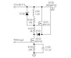
Looking at the partial schematic of my first attempt, we can examine the static conditions (Fig. 1). For dc, capacitors can be considered open circuits, and inductors can be considered short circuits. Consider first the case where the input PWM signal is steady low, at 0 V above ground potential. Q122 is thus off, and no current flows through its drain.
Q121’s gate is at VIn via R120. If the gate of Q120 is further below VIn than the gate threshold of Q121 (approximately 1.6 V to 2 V), then Q121 is turned on, pulling up the gate of Q120 smartly to VIn. Once Q120 gate rises within a volt or two of VIn, the rise is relatively slow, but we don’t care about that because Q120 is already in cutoff, as its gate threshold is about 6 V.
Next, examine the condition of steady-state “on.” The PWM waveform is high at 3.6 V. Q122 turns on, but only enough for current to rise to 10 mA. At this condition, R122 at 200 Ω has a drop of 2 V, placing the Q122 source at 2 V, so Vgs is right at the Q122 turn-on threshold of 1.6 V (the 3.6 V of the PWM voltage, minus 2 V at the Q122 source). Q122 then sinks 10 mA through its drain.
Current flows through R120 and R121 so the voltage across R121 rises to the gate threshold of Q121, turning it on just enough that the current adds to the current through R121 and R120 to equal the 10 mA being sunk by Q122. Since the turn-on threshold of Q121 is about 1.6 V, this condition will occur with about 1.6 V across R121. Current through R120 must equal that through R121, so we have a total of 9.6 V across R120 plus R121. Q120’s gate is now at 9.6 V, and Q120 is fully on, as we desire.
A Real Turn-On
But wait a minute. We said this was for a switching application, and we can get in deep trouble if the switching happens too slowly. To see why, consider the case of the MOSFET being halfway on. In the “off” case, we have zero current and thus zero power dissipation. In the “on” case, we have zero voltage and thus zero power dissipation in an ideal case. In practice the power dissipation is very low.
But in the “halfway on” case, at some point we are in the linear region of the device, where we have half the total voltage and half the total current at the same time, with 40 V × 10 A = 400-W dissipation. That much power is going to get pretty toasty very quickly, even with a decent heatsink. (Did you ever try to unscrew a 100-W incandescent light bulb while it’s on? Ouch!)
The key therefore is to switch quickly, so we don’t stay in that linear region very long. We would like to be able to pulse-width modulate this circuit rapidly (at 10 kHz to 100 kHz in my application). But we are limited by how often we can pass through the linear region, depending upon how much energy we dissipate in each transition. So, we want the transition to be fast. Q120 is big (to handle the main current), and its gate looks electrically like a relatively large capacitor as a result.
We must add or remove nearly 200 nanocoulombs (nC) to switch it between the on and off states. Recalling that an ampere is a coulomb per second, 10 mA requires 20 µs to add or remove 200 nC. Even if we switch at 25 kHz, we spend almost our entire time in the linear region. Even if we were to slow to 2.5 kHz, we would be spending almost 10% of the time in linear operation, which is not good.
How can we speed things up? In my first attempt, I added C122 specifically to speed up the turn-on. Starting with Q122 off and C122 discharged, we raise Q122’s gate to 3.6 V. Q122 stays fully on, with only 10-Ω resistance (it’s a fairly tiny SOT-23 FET, hence relatively high on resistance), until C122 rises to about 2 V and R122 takes over. Remarkable coincidence, of course: that happens about the time we have removed 200 nC of charge from Q120’s gate.
Actually, of course, I chose the value of C122 to achieve exactly this result. Ignoring the current through R122 during the very brief turn-on, the 200 nC of charge removed from Q120’s gate goes into charging C122, and 200 nC divided by 0.1 µF yields 2 V on C122. There is between 12 and 80 V across the string, limited only by the non-ideal resistances of the traces plus D121, Q122, and C122, so the instantaneous current will be greater than an amp.
Consequently, it takes less than 200 ns to bring Q120 fully on, which is 100 times faster than without C122. Note that L120 does not begin passing significant current during this charge time, so Q121 does not fight us. Inductor L120 is actually present for a different reason, but if you can’t fix it, feature it.
And A Turn-Off
Achieving a fast turn-off with a low steady-state bias current proved to be the trickiest part of this design. I explored quite a few different approaches before coming up with this one, where L120 comes into full play. Just before turn-off, approximately 1 mA is flowing through L120 to supply the current needed to drop 2 V across R121, placing Q121 gate at its 1.6-V threshold plus about 0.4 V being dropped in D121. When PWM voltage drops to ground, Q122 turns off crisply.
The current through L120 cannot change instantaneously, however. Current through R121 drops to zero because it has nowhere to go, being blocked by D121 and the now off Q122. Current into Q121 gate also goes nowhere, but sharply raises the Q121 gate up above Vin, to the point that D120 is forward biased and begins to conduct. Q121’s gate then stays at a diode drop above Vin, and Q121 turns fully on, pulling Q120 gate vigorously up to within about 1.2 V of VIn (Q121’s gate is 0.4 V above VIn, and Q121’s source is 1.6 V lower), guaranteeing that Q120 turns off very sharply.
At the instant of turn-off, Q121 turns fully on at 10 Ω with 10 V across it, so 1 A quickly drains off the Q120 gate charge to below the 6-V threshold. The current through L120 drops to negligible in about 200 ns due to the braking action of R120, and we return to quiescent “off” conditions.
PWM At The Extremes
But what happens with very short “off” times, where duty cycles are near but not quite at 100%? If the off time is very short, C122 does not have time to discharge. The combination of C122 and R122 has a 20-µs RC time constant, and it must discharge for several time constants. Thus, C122 does not provide the full “kick” for a fast turn-on.
Although I haven’t used perfboard in years, this seemed like a good circuit to prototype before committing to a printed-circuit board (PCB). It turned out that old-fashioned perfboard, the kind with copper rings around the holes, works out very well for typical surface-mount (SMT) parts. I also learned that short “off” times, which are likely in the intended application, are a problem and would greatly increase power dissipation in Q120.
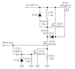
Figure 2 shows a modification of the basic circuit, with C122 replaced by another MOSFET to provide the turn-on “kick.” At the rising edge of the PWM waveform, C123 is discharged and acts as a short circuit, turning Q123 fully on and shunting R122 to ground. Q122’s source then turns fully on, providing a current burst to rapidly pull down on the gate of Q120 as described above.
C123 charges through R123, with an RC time constant of 3.9 µs. The gate threshold of Q123 is such that it takes only about one-fourth of the RC time constant to turn Q123 off, so we get about 1 µs of high current and then it drops back to steady-state conditions. When the PWM signal goes low, C123 discharges rapidly through D123 and is then ready quickly for the next cycle.
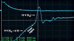
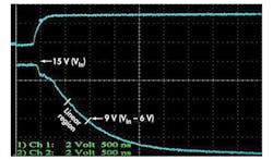
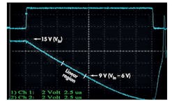
Figure 3 shows the turn-on waveform of the final circuit. The upper trace is the 3.6-V PWM signal. The lower trace is the resulting gate waveform on power MOSFET Q120. The initial sharp drop from the “off state” at 15 V is the turn-on of Q123, which is capacitively coupled through Q122 to the Q120 gate.
The signal then plateaus briefly until Q122 gets around to turning on and finally falls cleanly through the 11- to 9-V area (4 V to 6 V of Vgs on Q120) in about 400 ns. Compare this to Figure 4 of the same situation, but without the boost provided by Q123. In addition to the much flatter slope, note also that the horizontal scale has been compressed by a factor of 5. The actual transition takes almost 4 µs, or 10 times longer than with the Q123 boost!
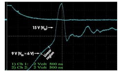
Figure 5 shows the corresponding turn-off waveform. We again get through the linear region in about 400 ns. I thought at first that the big overshoot afterwards was due to using too large an inductor, but the explanation is more subtle. The load I used on the output consists of about 6 feet (2 m) of wire going to a circuit-breaker panel and then another 6 feet of wire going to a lead-acid battery bank.
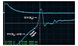
If I turn off the circuit breaker, the overshoot and subsequent ringing go away, so the overshoot and ringing come from the wiring (inductance) and the battery bank (capacitance and inductance). Removing L120 and replacing it with a short results in the waveform of Figure 6.
This waveform shows that the inductor provides somewhat less of a boost than I expected. The linear transition only increases to about 600 ns, and the slightly slower turn-off results in a bit less overshoot and ringing. The difference in the two waveforms, however, is subtle. Upon turn-off of Q122, current flow ceases through R121, so R120 pulls the Q121 gate smartly to VIn.
Q121 therefore turns fully on until its source terminal rises to within about 2.5 V of VIn, at which time Q121 begins to turn off. By then, however, Q120 has turned solidly off. We can actually trade off a slightly slower turn-off (600 versus 400 ns) for a slight decrease in bill of materials (BOM) cost and parts count (L120 and D120), depending upon the exact needs of the application.
This circuit provides a stable dc gate level squarely between the turn-on threshold and the absolute maximum of Q120 while dissipating only 10 mA in the quiescent condition. It pushes the Q120 gate through the linear region in a small fraction of a microsecond. The inductor is the most expensive component in the driver circuit, at 12 cents. The three FETs and three diodes are 4 cents each in quantity, and the remaining passives total under 5 cents in quantity, for a total bill of materials (BOM) cost of $0.41—good, fast, and cheap!
Steven P. Hendrix, P.E., has done embedded control design for some 35 years. He lives on the rim of the Cuyahoga Valley with his wife Kathy and five children, and sometimes foster children. He is also active in Boy Scouts and other volunteer activities. He can be reached at [email protected].
