Basic Guidelines for Mixed-Signal PCB Layout Design (Download)
A mixed-signal printed-circuit-board (PCB) design requires basic understanding of analog and digital circuitry to minimize, if not prevent, signal interference. Modern systems consist of components that are operational with both digital and analog domains, and they must be carefully designed to ensure signal integrity all throughout the system.
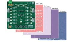
PCB layout—an important part of the mixed-signal development process—can be intimidating and component placement is just the beginning. Other factors must be considered, too, including board layers and how to properly manage them to minimize interference caused by parasitic capacitors that can be unintentionally created between the PCB’s interplane layers.
