64 Layers and QLC Push Flash Memory Technology Boundaries
Last month's Flash Memory Summit was host to a flurry of new flash memory product and technology announcements. Toshiba was talking about QLC (Quadruple Level Cell) BiCS Flash that promises to double capacity, storing four bits of information versus three bits for TLC and two for MLC flash memory. There is a corresponding reduction in the write lifetime just like the differences between SLC, MLC, and TLC memory, but the higher density will be ideal for applications where read operations occur much more often than write. This type of memory will likely fill in the higher niche of a memory hierarchy that is becoming more common and complex. Production of QLC flash memory is still in the future.
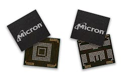
In the meantime, there are products that will be showing up a lot sooner, including Micron's first products based on the Universal Flash Storage (UFS) 2.1 standard (Fig. 1). These 32-Gbyte mobile devices target the mid- to high-end smartphone market where performance is important. They utilize high-speed serial interfaces, as opposed to the parallel interface of eMMC that will be edged out as UFS comes online. The eMMC flash memory will still be used, especially in embedded applications where high performance and capacity are not as important as cost and ease of interfacing.
Micron's USF chips utilize the company's 3D NAND technology. The die is only 60.217 mm2. Micron also supports multichip packaging (MCP) that combines 3D NAND with LPDDR4 memory for a compact, low-power solution ideal for high-end mobile devices.
Multilayer flash memory devices continue to push the capacity boundaries. Samsung was highlighting its 64-layer V-NAND. Last year, the company was talking about tis 48-layer V-NAND chip MLC chip with a 256 Gbyte capacity. The latest 64-layer dies hold 512 Gbits of TLC storage so a single 11.5-mm by 13-mm BGA SSD chip will be able to store 1 Tbyte. Look for 4 Tbyte M.2 devices in the standard 22-mm by 110-mm form factor. A non-standard, 32-mm by 114-mm module could double the capacity. This will likely turn into an M.2 server form factor where the higher capacity is advantageous.
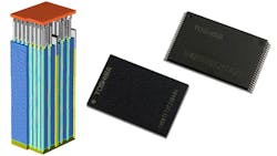
Not to be outdone, Toshiba and Western Digital partnered to develop their 64-layer flash memory device (Fig. 2). These use Toshiba’s BiCS TLC technology and will provide 512 Gbits of storage. The flash memory devices will be used in products from Western Digital and its recently acquired SanDisk brand.
Stacked memory has brought significant gains in capacity, and memory designers will continue to push the limits. The challenge is to continue to scale the manufacturing process that is already quite challenging. The through-silicon-via (TSV) technology continues to improve but, like die designs, there are limits.
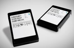
One alternative is to stack the stacks. Multiple chips are already used in solid-state drivers (SSD). Samsung was demonstrating a 32-Tbyte, 2.5-in SSD (Fig. 3), while Seagate was showing a 60-Tbyte drive that had a 3.5-in form factor. 100-Tbyte drives are forecast for 2020.
Capacity continues to dominate the storage discussion, although cost and lifetime remain key issues. The range of options can be extremely confusing even for embedded applications with more specialized form factors, rugged requirements, and features like Virtium's self-encrypting drives. These SSDs bring enterprise encryption to embedded applications.
Developers will need to balance all these options when designing a system. On the plus side, putting high-capacity, high-performance storage on a board is a lot easier now. Not all form factors or interfaces will be applicable to a particular design, but there will likely be a large selection of devices that will deliver the necessary capacity, performance, and security for the right price.
About the Author
William G. Wong
Senior Content Director - Electronic Design and Microwaves & RF
I am Editor of Electronic Design focusing on embedded, software, and systems. As Senior Content Director, I also manage Microwaves & RF and I work with a great team of editors to provide engineers, programmers, developers and technical managers with interesting and useful articles and videos on a regular basis. Check out our free newsletters to see the latest content.
You can send press releases for new products for possible coverage on the website. I am also interested in receiving contributed articles for publishing on our website. Use our template and send to me along with a signed release form.
Check out my blog, AltEmbedded on Electronic Design, as well as his latest articles on this site that are listed below.
You can visit my social media via these links:
- AltEmbedded on Electronic Design
- Bill Wong on Facebook
- @AltEmbedded on Twitter
- Bill Wong on LinkedIn
I earned a Bachelor of Electrical Engineering at the Georgia Institute of Technology and a Masters in Computer Science from Rutgers University. I still do a bit of programming using everything from C and C++ to Rust and Ada/SPARK. I do a bit of PHP programming for Drupal websites. I have posted a few Drupal modules.
I still get a hand on software and electronic hardware. Some of this can be found on our Kit Close-Up video series. You can also see me on many of our TechXchange Talk videos. I am interested in a range of projects from robotics to artificial intelligence.


